I'm toying with a compact (60x38mm) layout for a blameless kind of amp, with cfp outputs.
Right now, I've got a zobel network going from the output track to the ground pin of a decoupling cap tied to the negative rail (C5-R7)
I could duplicate the RC network to the other side of the output track, doubling the resistance and halving the capacitance, which would have some advantages in terms of parts (I can use smaller caps to start with). But would that hinder the zobel operation ?
Thanks in advance for any clarification on this. 🙂
Attachments
I think it not a good idea, you will create a new path and it will build a loop; ( from ground on one side, through zobel 1, then zobel 2, and ground on the other side ) and I think il could go in oscillation. But I must admit resistors used in zobel circuit will damp oscillations a lot .
Thanks for the comments. The main consideration is that the biggest smd polyester cap of sufficient voltage rating I can fit in there is 47nf, 1812 package. Two networks means an equivalent 100nf. No big deal but I was curious about possible trouble in doing so.
Bob Cordell's book talks about splitting the Zobel into two (R series C) networks, one on either side of the output inductor. And the Cordell Audio website page that describes his Super Gain Clone chipamp, includes an enigmatic little tidbit, attached below:
_
_
Attachments
Distributed Zobel networks are an excellent idea. Best would be to place one at each output stage transistor, connected to the emitter. This gives the shortest current loop and most effective Zobel in case you manage to implement this well on the PCB, which means you have at least two layers, better four layers PCB and route ground short and thick.
Since power dissipation in the Zobel resistor may be substantial, distributed Zobel networks also helps to dissipate power.
Calculation goes as you did.
A second Zobel after the output inductor is another thing.
In my latest output stage, I used both distributed Zobels and a secondary Zobel after the inductor. The distributed Zobels survived front end related oscillation well despite each having only 0.6W power rating. The secondary Zobel resistor burned and I had to put a far more powerful on the PCB instead.
Make sure that resistors are capable of handling a lot of power in case the amp oscillates during debug. If they fail, oscillation becomes even worse.
Thanks for the suggestions and also simply for the term "distributed zobel", I found some hits on the forum with that keyword, mostly from Bob Cordell.
The resistors I'd use would be 3W thick film resistors, datasheet here, same as for the emitter resistors. The caps are 100Vdc, PET caps. The amp is intended for about 30-35V rails.
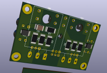
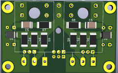
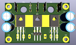
The attached images show the starting point. The top layer will be all ground. The three to126 are the cfp drivers thermally linked to the vbe multiplier (they will all be clamped together). The input stage sits on another small pcb. The spades are v+, power gnd, out, gnd return, v-.
Under the board, the left and right planes are the power rails. r7/c5-r8/c6 would be the zobels, r1 to r6 are the emitter resistors, d1,d2 the catching diodes.
I guess I could tighten the loops a bit by moving the zobels to the side and taking the pickup point from the middle emitter resistor.
edit: or maybe would it be better to flip the zobels around and return these to the ground spades rather than to the decoupling caps ?
The resistors I'd use would be 3W thick film resistors, datasheet here, same as for the emitter resistors. The caps are 100Vdc, PET caps. The amp is intended for about 30-35V rails.
The attached images show the starting point. The top layer will be all ground. The three to126 are the cfp drivers thermally linked to the vbe multiplier (they will all be clamped together). The input stage sits on another small pcb. The spades are v+, power gnd, out, gnd return, v-.
Under the board, the left and right planes are the power rails. r7/c5-r8/c6 would be the zobels, r1 to r6 are the emitter resistors, d1,d2 the catching diodes.
I guess I could tighten the loops a bit by moving the zobels to the side and taking the pickup point from the middle emitter resistor.
edit: or maybe would it be better to flip the zobels around and return these to the ground spades rather than to the decoupling caps ?
Attachments
Last edited:
I have the term "distributed Zobels" from Bob's book.
The PCB design looks good. I would route the Zobel grounds to the spades. This is where all comes together in the end, kind of star point.
The PCB design looks good. I would route the Zobel grounds to the spades. This is where all comes together in the end, kind of star point.
3W SMT resistors need a large area of copper devoted to their heatsinking, otherwise you just have a 0.5W resistor that's rather larher than needed.
I found when testing a amp using high freq and amplitudes stresses the zobel components. Be careful. I would rather use the tried and true mox resistors, min 3w, if you can use fkp or mkp 100v min film caps too.
You don't think the wima PET are sufficient ? SMD-PET capacitors - WIMA – Competence in Capacitors
In his book, Cordell suggests C0G caps. Any opinion on this ?
In his book, Cordell suggests C0G caps. Any opinion on this ?
I can't see anything wrong with your caps.
NP0 / C0G would be a good choice as well.
Mark is right about the cooling of the SMT resistors. Better enlarge planes attached as much as possible.
NP0 / C0G would be a good choice as well.
Mark is right about the cooling of the SMT resistors. Better enlarge planes attached as much as possible.
- Home
- Amplifiers
- Solid State
- Splitting an output zobel in two, bad idea ?