The instructions were last used for IPC class 3 products so tented via's were not allowed. There is a wealth of information on the net both for and against tented via's, we do both and over the last 28+ years I have used both depending on the customers requirements, in normal day to day commercial and industrial products never noticed any difference or any long term problems with either tented or un-tented. That said it is becoming common practice to have a small opening in the solder resist over a via, about 0.1mm over the finished hole size, so a 0.3mm finished via (0.6mm pad) would have a 0.4mm opening on the solder resist. This also gives maximum solderability while allowing open vias. The worry is that processing chemicals can be trapped in the barrel and may in certain conditions become active and cause damage to the barrel plating, thus compromising the functionality of the device, not what you want on IPC class 3/3A assemblies.
What is IPC class 3, very simple explanation:
SolderTip #39: Class 2 vs Class 3 Assemblies | EPTAC
What ever method you decide on wont make any difference so go for the easiest, tented.
What is IPC class 3, very simple explanation:
SolderTip #39: Class 2 vs Class 3 Assemblies | EPTAC
What ever method you decide on wont make any difference so go for the easiest, tented.
Question about through pads:
When I specify a through pad in Sprint Layout with 0.65mm center hole, will the final air opening (through which the component lead will pass) be 0.65mm, or will it be 0.65mm-2x(plate track width)? 😕
In short, where does the centre hole refer to? Final air opening, or mechanical drill diameter which will be in turn plated?
It is the drill size. it is up to you to find out the plating thickness and choose drill size accordingly.
Thanks!
For Seeed, I read somewhere that it is the final hole, since they rearrange the drills in the fab after they take them from your gerber files, to account for the plating thickness too.
So I e-mailed them about that just to be sure. 🙄
For Seeed, I read somewhere that it is the final hole, since they rearrange the drills in the fab after they take them from your gerber files, to account for the plating thickness too.
So I e-mailed them about that just to be sure. 🙄
Specify finished hole size, you cant use the plating thickness as a guide to drill size. On average plating thickness is 0.025mm so for a 1mm hole you would expect a drill size of 1.05mm, in fact the manufacturer will more likely use a 1.1mm drill as the material relaxes after drilling.
So you always specify a finished hole size and let the manufacturer chose the correct drill size for both the laminate and their processing.
So you always specify a finished hole size and let the manufacturer chose the correct drill size for both the laminate and their processing.
I think this was once common, though not universal, and now rather rare. The PWB fabricators I've used over the last decade or so do NOT spec holes like this.It is the drill size. it is up to you to find out the plating thickness and choose drill size accordingly.
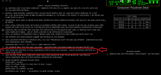
This seems to be the most common practice by far. Drawings I have done for commercial products explicitly call out finished sizes (see atch). (Of course, drawing notes only get read about half the time. 🙁 )Specify finished hole size, . . . So you always specify a finished hole size and let the manufacturer chose the correct drill size for both the laminate and their processing.
Dale
Attachments
I think this was once common, though not universal, and now rather rare. The PWB fabricators I've used over the last decade or so do NOT spec holes like this.
Over 28 years as a professional PCB designer, and I have never done it this way, I have always specified finished hole size.
Nearly PCB manufacture is governed by IPC specifications, for drill holes it is IPC-6012A.
3.13 Hole Size Tolerances
Hole size tolerances for all plated and non-plated shall be as shown below.
< 1.00mm +/-0.05mm
>1.00mm <2.50mm +/-0.10mm
>2.50mm +/-0.15
IPC-6012A 3.4.1 Hole size tolerance and hole pattern accuracy shall be as specified in the procurement documentation
Could someone help me to identify the problem with drillings on my layout? When I create drill file in Sprint, it says 239 drillings on the silkscreen layer and they will be ignored. As a result, exported drill file have all drillings in one corner of PCB.
Also, how to save in Gerber files cut out area in ground plane? In Sprint the layout is fine with applied cutouts, in gerber all cutouts disappeared.
Thanks.
Also, how to save in Gerber files cut out area in ground plane? In Sprint the layout is fine with applied cutouts, in gerber all cutouts disappeared.
Thanks.
- Home
- Design & Build
- Software Tools
- Spint Layout into Gerber