FET's work really for line level switching if the implementation is right, posts #2 and #201
http://www.diyaudio.com/forums/soli...fet-amplifier-designed-music.html#post1452488
http://www.diyaudio.com/forums/soli...-amplifier-designed-music-11.html#post1569428
http://www.diyaudio.com/forums/soli...fet-amplifier-designed-music.html#post1452488
http://www.diyaudio.com/forums/soli...-amplifier-designed-music-11.html#post1569428
Hello,
I would use something like an SSM2404.
It is an analog electronic switch.
In my opinion it is among the best.
It is made by Analog Devices.
Good Luck.
I've seen these mentioned many times but they are old and obsolete. You can still get them on eBay but I was hoping to find something newer and perhaps better!
FET's work really for line level switching if the implementation is right, posts #2 and #201
http://www.diyaudio.com/forums/soli...fet-amplifier-designed-music.html#post1452488
http://www.diyaudio.com/forums/soli...-amplifier-designed-music-11.html#post1569428
Interesting, Mooly. Did you use this method yourself?
Interesting, Mooly. Did you use this method yourself?
I did, and found it works extremely well.
I've found a number of ways to perform analog switching, among the highest performance a sort-of hybrid approach in which the junction of different input and feedback resistor pairs are switched at the inverting input of a given opamp. The advantage is that the opamp's input impedance is relatively high, so there is very little current through the switching element, most likely a JFET. So distortion mechanisms associated with JFET on-resistance variations with signal current are mostly eliminated. As well there is little common-mode swing and hence little common-mode distortion from the opamp.
Isolation can be quite good, as it depends on the ratio of the input + feedback R to the output impedance of the opamp. Of course this will degrade with declining loop gain with frequency. An additional shunt switch to common for a given unselected source, at the junction of input and feedback R, can improve the isolation even further. This is especially helpful when the capacitances of the off switches otherwise couple to the inverting input.
The disadvantage is that the opamp must drive a plurality of input/feedback networks, or even worse potentially with the shunt switching, so the requirements on output current are increased. There is also somewhat higher noise gain; for equal input and feedback values, hence unity gain for a given selected source, the noise gain for opamp voltage noise is two for a low-impedance source. And there will be resistor thermal noise, with the usual tradeoff of source loading versus noise. There is also a polarity inversion which needs to be accounted for.
As usual a picture would be helpful, so perhaps I'll draft one as a followup.
Brad
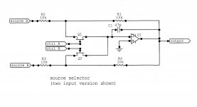
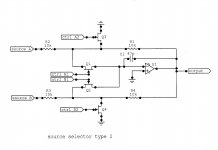
schematics
Examples are for two inputs, but can be expanded indefinitely based on constraints of the opamp output current capability.
The second type includes shunt switches. To select source A, ctrl A1 is at zero and ctrl A2 is biased negative, while ctrl B1 is negative and ctrl B2 is at zero.
Distortion is primarily determined by the opamp. Isolation at 20kHz for the type 1 neglecting strays is predicted to be about -116dB (better at lower frrequencies). For type 2 this improves to a predicted (and unlikely with strays) ~-160dB. For these simulations I used 2N4392 JFETs and an LM833. The off bias was -15V, which is adequate for +/- 10V peak input signals.
Attachments
Bcarso.
can you confirm that the left pic has noise at the mixer determined by the two paralleled 10k on each input?
Does the right pic have less noise because one of the 10k pairs is shorted to signal ground?
Can the difference in noise be measured or heard? Or is the noise of both so low that it is irrelevant for us?
noise
So at the end of the day, whether these contributions are negligible depends on the noise in the sources. One can make the circuit contribution smaller by making the resistors smaller, but this may load the sources unduly. Each input resistor can then be preceded by a low-noise unity-gain buffer, but clearly the complexity burgeons. And the buffers must themselves be happy supplying the higher signal currents, although load current compensation can be used to reduce potential distortions, with even greater complexity!
For the second (right-hand) circuit the isolation between channels is enhanced by the grounding of the unselected resistor pair's junction. The noise situation does not change because again the unselected resistors are disconnected from the opamp inverting input.
Note that for the first circuit, the worst-case requirements on the opamp's output current occur for the fairly pathological case of one channel swinging maximally with one polarity and the other maximally with the opposite polarity.
The noise analysis is straightforward for both circuits. To be clear, this is a source selector and not a mixer --- only one input is selected at a time. For the first circuit, for the unselected input there is no contribution to noise since the given JFET disconnects the input and feedback resistors. The selected channel has the resistors' noise contribution of about 18.2nV/sq rt Hz, thus in a 20kHz bandwidth the output noise contribution will be about 2.57uV at nominal room temperature. The opamp's e sub n, including 1/f noise at lower frequencies, will be amplified by a factor of 2. Opamp input parallel ("current") noise will be converted to an output noise voltage via multiplication by the feedback R of 10k. For a JFET amp this can be ignored, for some low voltage noise bipolars it must be included as their parallel noise can be quite high.Bcarso.
can you confirm that the left pic has noise at the mixer determined by the two paralleled 10k on each input?
Does the right pic have less noise because one of the 10k pairs is shorted to signal ground?
Can the difference in noise be measured or heard? Or is the noise of both so low that it is irrelevant for us?
So at the end of the day, whether these contributions are negligible depends on the noise in the sources. One can make the circuit contribution smaller by making the resistors smaller, but this may load the sources unduly. Each input resistor can then be preceded by a low-noise unity-gain buffer, but clearly the complexity burgeons. And the buffers must themselves be happy supplying the higher signal currents, although load current compensation can be used to reduce potential distortions, with even greater complexity!
For the second (right-hand) circuit the isolation between channels is enhanced by the grounding of the unselected resistor pair's junction. The noise situation does not change because again the unselected resistors are disconnected from the opamp inverting input.
Note that for the first circuit, the worst-case requirements on the opamp's output current occur for the fairly pathological case of one channel swinging maximally with one polarity and the other maximally with the opposite polarity.
bcarso, nice tutorial.
A lot cheaper than relays, but other than isolation, how does the ckt perform!!If you have done a sim or actual testing, I'd be interested in the results?
Thx
And a lot faster than relays, with no concern about contaminated contacts. Actually that latter is probably the main attraction for me. Otherwise metal on metal is nearly ideal.
I've used similar techniques in the past with real parts with success. With the sims, the isolation results are as stated, with the stated caveats. The distortion performance also sims ridiculously well, beyond the capability of analyzers, as would be expected based on the configuration that essentially removes all of the switch variation with signal at audio frequencies. Again, the opamp will likely be the limiting factor, especially if it is challenged based on output demands.
One thing I didn't mention is that, at some point, we may have concern, with a sufficiently high on-resistance of the switch, as its thermal noise adds directly (uncorrelated) to e sub n of the opamp. For medium-length channel parts like the old process 51 this is of order 30 ohms, depending on pinchoff voltage, so for the vast majority of opamps this will be negligible. If instead some high-voltage CMOS bilateral switches (like the 4016) are used, we get into some grey areas on noise. Still, won't be too bad for most situations.
You perked my interest. I have a 5.1 analog/digital pre-amp design that I have in the works. You name it, I put it on the pcb. Never made it yet because of cost. Relays were a huge expense, just like any switches are. I was planning on up to maybe 8 channels to be switched analog. Might be done in a mux fashion. 8-4-2-1
If the opamp is the limiting factor, then the whole design is squashed, as there are a lot more of them")
If you draw up a test ckt, even if is in LTspice(preferred), i'll convert to Orcad, lay it out, fab, test. Prefer SMT, just cheaper on pcb area. BF862 (preferred) and common opamp foot print so-8. Maybe even throw on a PGA2320, connectors and actually make a small pre-amp, or something a little more useful. Lots of possibilities We can start a new thread as well if it is req.
If the opamp is the limiting factor, then the whole design is squashed, as there are a lot more of them
If you draw up a test ckt, even if is in LTspice(preferred), i'll convert to Orcad, lay it out, fab, test. Prefer SMT, just cheaper on pcb area. BF862 (preferred) and common opamp foot print so-8. Maybe even throw on a PGA2320, connectors and actually make a small pre-amp, or something a little more useful. Lots of possibilities We can start a new thread as well if it is req.
If you could detail the requirements that would be a good starting point. In particular the voltage swings are important for determination of the specific switch element needs, including the breakdowns and gate drive details. 862s are nice parts but do have some limitations. They are nice in having a low pinchoff voltage though. In the circuit examples shown the gate of an off part has to be at least a little negative with respect to either channel connection. The second version is best for breakdown as the shunt switch keeps the unselected channel's resistors close to common. The other nice thing about the circuit is that the switches are fairly well protected against overvoltage/overcurrent by the resistors.You perked my interest. I have a 5.1 analog/digital pre-amp design that I have in the works. You name it, I put it on the pcb. Never made it yet because of cost. Relays were a huge expense, just like any switches are. I was planning on up to maybe 8 channels to be switched analog. Might be done in a mux fashion. 8-4-2-1
If the opamp is the limiting factor, then the whole design is squashed, as there are a lot more of them
If you draw up a test ckt, even if is in LTspice(preferred), i'll convert to Orcad, lay it out, fab, test. Prefer SMT, just cheaper on pcb area. BF862 (preferred) and common opamp foot print so-8. Maybe even throw on a PGA2320, connectors and actually make a small pre-amp, or something a little more useful. Lots of possibilities We can start a new thread as well if it is req.
Another detail is the likely requirements on what the opamp outputs drive. And, to what extent specific timing of the control voltages is needed to alleviate switching transients.
Anyway, it would be interesting to see something built, say starting with a given cell.
Brad
Hi Brad and others,
I like the second version as well.
Usually a dual supply of min +/- 15V, since this is what the PGA2320 has. Dynamic range is always a ? Originally I chose PGA2320, but could change to Cirrus 3318 which is +/-9V. I have heard good reviews for this part and it is small footprint for a 5.5/7.1 implementation.
OPAMP drive is >600ohm.
Switching control will be in the from a 3.3V I/O MCU or I2C port digital control. Well maybe a DAC would be better, for a gradual switching (ramp)? the Atmel xmega MCU has 2 DAC's. Lots of I/O's for control. So will obviously need level shifters made out of discrete elements.
Since the MCU has control over switching and volume, ramping will be done in SW.
I am using a MAX9729, on a portable unit, , even at 3.3V supply it works very well. But I do measure its distortion and it is as stated in the spec's 0.03%. Also uses a TPA3100D2 PA in the portable unit.
Rick
I've been looking at the drive requirements for the second circuit and realized that the voltage swings at the gates can be drastically reduced compared to the first circuit, which by itself is a big enhancement.Hi Brad and others,
I like the second version as well.
Usually a dual supply of min +/- 15V, since this is what the PGA2320 has. Dynamic range is always a ? Originally I chose PGA2320, but could change to Cirrus 3318 which is +/-9V. I have heard good reviews for this part and it is small footprint for a 5.5/7.1 implementation.
OPAMP drive is >600ohm.
Switching control will be in the from a 3.3V I/O MCU or I2C port digital control. Well maybe a DAC would be better, for a gradual switching (ramp)? the Atmel xmega MCU has 2 DAC's. Lots of I/O's for control. So will obviously need level shifters made out of discrete elements.
Since the MCU has control over switching and volume, ramping will be done in SW.
I am using a MAX9729, on a portable unit, , even at 3.3V supply it works very well. But I do measure its distortion and it is as stated in the spec's 0.03%. Also uses a TPA3100D2 PA in the portable unit.
Rick
I'd recommend not attempting any ramping of the gate drives. What emerges from a study of the switching behavior is the need to provide a small overlap of series switching and a definite turnoff of the shunt switching (you don't want the opamp's input tied to common ever). Probably the simplest adequate approach is with schottky diode/R/C arrangements at the inputs of inverter gates like in the 74AC04, driven from simple discrete common-base stages, those in turn from a serial-in parallel-out register fed from the uC. The inverters would be powered from 0V for Vdd and about -3V for Vss, the discrete level shifters ahead of those, and from there on back everything standard 3.3V stuff. The register would clock all of the parallel outputs at once with minimum skew.
Or, something else altogether
It kind of depends on one's preferences --- a lot of folks would do all the timing in the uC, but for me the surety of the fast timings involved favors the arrangement outlined.Although the aim here is to provide source switching with minimal glitch energy, the composite system with the programmable gain block and uC could of course mute between selections and remove concerns for the most part about switching transients.
If the PGA part or ~equivalent is used it's what will determine outside world drive anyway, and its own input impedance is I think pretty high. As discussed the choice of 10k nominal resistances is a tradeoff of source loading versus noise. For a higher-performance approach I'd use smaller R and buffering ahead, but parts proliferate rapidly. If one uses the circuit with one of the recent fashionable opamps like the LME49990 the parallel noise is the dominant contribution (2.8pA/sq rt Hz * 10k = 28nV/sq rt Hz). Using an opamp with lower parallel noise and higher voltage noise is probably more optimal. Another option is prefacing the ~49990 with a BF862 source follower (adding its voltage noise but rendering parallel noise of the opamp insignificant), or with greater effort spinning a hybrid amp with JFET input with gain and a ~49990, with more parts and lots of care needed to avoid instability. And with the single discrete JFET one worries about offset voltage and drift. In any case with the simple opamp the performance will still be better than most sources.
I'll get round to publishing what I've got in mind for the gate drives pretty soon, after I figure out how I'm going to fund October
Of course anyone else is welcome to jump in with thoughts and suggestions.Also, if anyone has seen something like this approach I'd be very happy to acknowledge prior art. I'm having some discussions with an ex-console designer and an RF guy and others on Facebook, where I reproduced the schematic. But so far something that looks identical hasn't turned up. There are lots of prior circuits using opamps and switches in which a first-order compensation for on resistance is done with a similar switch in the feedback. But the above circuits have to be out there somewhere, probably in several appearances.
Yes, priorities trump foolin around stuff. As it is, am just adding onto my pile of experimentsI'll get round to publishing what I've got in mind for the gate drives pretty soon, after I figure out how I'm going to fund October
Yes I would think this would be the case. Usually you like to gain match your sources.Although the aim here is to provide source switching with minimal glitch energy, the composite system with the programmable gain block and uC could of course mute between selections and remove concerns for the most part about switching transients.
These PGA parts need low source impedances so a buffer is needed from the source side.
A discrete jfet opamp is fine with me, I have a 10x LSK389B that I was going to use in the phono section, Denis Colin clone or Low Noise Design Schematics (HPS2.0)
How about a jfet opamp TI OPA164x?
A hybrid opamp as Sansui au-x911dg has done, for the MM phono. Sch too large for upload
I see 12k "typical" on the datasheet and 18pF. That's quite within the capabilities of most any opamp used in the source selector (net peak current required for a 10V peak signal of 8.8mA, when 10k resistors are used for the source selector and all eight are stuffed).These PGA parts need low source impedances so a buffer is needed from the source side.
Looking at the JFET switch drives, it looks like a part like the -AHC595 could be run with the 0V/-3V rails as well, and the discrete level shifting from the 3.3V uC done with just three lines, one data and two clocks. Have to see if a single AC04 gate can drive all of a group of series or shunt JFET gates (probably fine). The 595 has an output register that is clocked independently, so skew will be small.
- Status
- This old topic is closed. If you want to reopen this topic, contact a moderator using the "Report Post" button.
- Home
- Source & Line
- Analog Line Level
- Source selector using Analog switches or multiplexers - opinions?