Hi all, I've got an older Sony 2 channel receiver that I'd like to keep going, as it sounds great, and we don't need more than two channels anyway. Picked this unit up for cheap second hand a while back, and it worked well for a while before it started acting up.
I've narrowed it down to one of the amp(pre-amp?)transistors, but seeing as I'm fairly noobish still when it comes to troubleshooting electronics, I wanted to run it by anyone familiar with amp circuits, and see if anyone had any input as to what exactly might have caused the failure.
Symptoms:
Unit goes into protect mode if left on overnight. Cycling power clears protect mode. Left channel is a clipped static sound. I.E. only the high volume parts of the sound come through as a sort of static.
Troubleshooting and elimination:
Eliminated the main amp transistors via testing and swapping them. Worked when reassembled, so thought perhaps it was a bad solder joint. Failed again within a day or so, same channel.
Took a closer look at the board, and found a couple dark areas and what seemed to be visibly failing solder joints. Re-soldered joints, same problem.
I then started pulling and testing the transistors in this darkened patch, and finding no faults I swapped channels when re-installing them. Bingo! The problem switched channels. It would seem it is one of the 2SC2958 transistors.
The 2sc2958 and 2sa1221 pairs get very hot to the touch.(Hard to touch them for more than a couple seconds, and when I put an alligator clip on one it got warm). Hot enough to brown the board, and also cause at least partial failure of the solder joints. The 2sc2958 on the left channel seems to be the failing component. The left channel also has a darker 'burnt' area from the heat than the right.
Questions:
1)Is it likely that they've been getting this hot for the life of the unit, and it's just now failing from the effects of the heat? Or is another component failing causing the transistors to overheat? (These are getting hot to the touch without any input or output happening. No speakers hooked up. No inputs. Just sitting there turned on.
2)Which other components are the likely candidates for causing this problem, if any?
3)The small arrows with numbers on the schematic are indicating voltages, correct? How far off is acceptable variation? (I've seen 1 volt maybe a bit more variations from what's printed on the page).
Any help you can be would be great. I hope this is acceptable to post here. If there's a better forum for this, please let me know. Seems like a good project to learn some things on. It's fairly simple being 2 channel, it's easy to pop open and work on without much dis-assembly, and it puts out some pretty good sound. I figured I'd try to learn a bit more, and save some money at the same time. I've got the time to troubleshoot it.
Thanks!
(click to enlarge - pics embedded via imgur - let me know if they're not visible)
Last edited:
You've done really well to get this far 🙂
A word of caution... don't risk using your speakers on it until the fault is fixed. For some peculiar reason (I mention this many times) Japanese transistors of the type used for drivers etc as here often fail by going intermitent open circuit.
Discoloured "paxolin" type PCB is absolutely normal with heat. All I think you need do is to replace the transistors. I'd perhaps go for something like the MJE340 and MJE350 and replace all four. Different package so you would have to identify the leadouts and fit accordingly.
When powering up we always recommend a "bulb tester" (search the forum) to prevent any damage if things are amiss.
There are two checks on any amp. One is that there is no DC offset at the output and the other is the output stage quiescent current. I see this is a fixed bias design... hmmm... no problem 😀
More on the fixed bias...
Look at R802 and R852 which are unmarked. These will be adjusted on test to give the appropriate bias to the output stage. I would advise that you measure and record the tiny DC voltage across the 0.22 ohm resistors (no signal and no speakers) both for interest and for reference. I would guess around 20 millivolts when the amp is warm.
Look at R802 and R852 which are unmarked. These will be adjusted on test to give the appropriate bias to the output stage. I would advise that you measure and record the tiny DC voltage across the 0.22 ohm resistors (no signal and no speakers) both for interest and for reference. I would guess around 20 millivolts when the amp is warm.
check q706 for operation but mostly shorts to heatsink.
Don't worry about the accuracy of measured voltages. 1 volt difference from the specified value is probably ok, but some are more important...!
what is the DC offset voltage on the outputs ?
Don't worry about the accuracy of measured voltages. 1 volt difference from the specified value is probably ok, but some are more important...!
what is the DC offset voltage on the outputs ?
Thanks very much for the input and the tips guys.
What are the thoughts behind moving to the MJE340/MJE350 combo? Also, I'd heard that changing components could change the bias? Would this be an issue?
Where would the r802/r852 be located? I'm having difficulty finding them.
DC offsets on output:
Left channel(was the failing channel, but transistors were swapped) Seems to fluctuate/bounce between ~3 and ~5.5 mV.
Right channel(now contains what would seem to be the faulty transistor) Fluctuates between ~1 and ~3 mV. (seen it drop to negative a couple times).
I touched these transistors again after letting it sit on for a bit, and the heat they're putting out is at the "feels like it burnt you after a split second" levels. Seems like at the very least, they could use some heat sinks if possible.
First thing - change all those small electrolytics. The ones I'd look at first are C701, C751, C708, C758 as these are in the signal path. Also C727 as it is decoupling for the VAS and small signal stages of both channels.
I would not change those transistors for MJE340/350. Q707/757 is the VAS stage for this amp, so changing it will change stability criteria.
I would not change those transistors for MJE340/350. Q707/757 is the VAS stage for this amp, so changing it will change stability criteria.
R802 and 852 are located directly above Q707 and Q757
The DC offsets are fine but they could alter when the fault appears. Did you measure the voltage across those 0.22 ohms ? Changing any semiconductors in the output stage could affect the bias. That's why its worth measuring it now to see what it is set at. Its no big problem getting the bias optimal anyway, its just interesting to see/check/confirm what it is now.
Do the transistors that you say get hot differ much in apparent temperature compared to the good channel ? You could carefully measure the volt drop across resistors R713and R716 in one channel and R763 and R766 in the other to compare. They are the 22 ohm resistors that go to these drivers.
Jaycees' not keen on the MJE's but I think they would be a good choice. They are heavily "slugged" by the 68pf caps across B-E of each. I think they would be fine 🙂
Hmm. It appears that R802 and R852 were never installed in this board. Found their locations, but they're empty. Shiny patches of solder. Apparently bias adjustments weren't needed?
The .22 ohm resistors are dropping 3.2 mV (R ch) and 2.5 mV (l CH). There is only about 4.5 mV max at any point on these.
As far as the heat issue, both channel pairs are very similarly hot to the touch.
Tested the drop across 22 ohm resistors, they seem to be very close to each other. One might be off by about 10 mV, but that's about it.
Any more than 5mV will cause the protection to operate.More on the fixed bias...
Look at R802 and R852 which are unmarked. These will be adjusted on test to give the appropriate bias to the output stage. I would advise that you measure and record the tiny DC voltage across the 0.22 ohm resistors (no signal and no speakers) both for interest and for reference. I would guess around 20 millivolts when the amp is warm.
Check that there is around 3mV or less across one of the 0R22 resistors on the emitters of the output transistors. If there is any more, adjust the bias pots.
Hmm. It appears that R802 and R852 were never installed in this board. Found their locations, but they're empty. Shiny patches of solder. Apparently bias adjustments weren't needed?
The .22 ohm resistors are dropping 3.2 mV (R ch) and 2.5 mV (l CH). There is only about 4.5 mV max at any point on these.
As far as the heat issue, both channel pairs are very similarly hot to the touch.
Tested the drop across 22 ohm resistors, they seem to be very close to each other. One might be off by about 10 mV, but that's about it.
If those resistors aren't fitted then it just means the correct bias could be achieved with a single value resistor. Two in parallel allows a much wider range if a single standard value part isn't quite right. Normally (as in 99% of designs) a preset would be fitted there for manual adjustment.
3.2mv is around 15 milliamps quiescent current. Its much lower than I expected for an EF (emitter follower) output stage. That value would have to be checked/confirmed after replacing the drivers and if necessary the value of one of the resistors altering... all easy stuff. It may not need any action anyway... but it must be checked.
Similar current in the 22 ohms and similar heat in all the driver transistors is going to be normal for this amp.
I would just replace all four driver transistors.
Any more than 5mV will cause the protection to operate.
Check that there is around 3mV or less across one of the 0R22 resistors on the emitters of the output transistors. If there is any more, adjust the bias pots.
The bias current has no effect on DC offset (and it is DC offset that causes the protection to operate).
1 milliamp or 1 amp, the offset stays the same.
Thanks again for all the input and info, guys.
The manual calls for 2SC2958-L and 2SA1221-K's. What do these suffixes mean? Did a web search, but haven't come up with anything concrete. Are these differences in pin-out or something?
If I were to just replace them with the same transistor, would these be correct?
2SC2958 - B&D Enterprises International
The 2Sxxxx is a numbering system. 2SC are NPN and 2SA are PNP. The L suffix could be some "in house" grouping such as gain etc.
You need a "complementary pair" (such as the MJE340 and 350 I mentioned). Always buy semiconductors from a reputable supplier. Huge number of fakes around from well known auction sites.
Look up the devices and the pin outs here. Just type the main device number (such as 2SC5958) in the blank box and search.
Datasheet catalog for integrated circuits, diodes, triacs, and other semiconductors, view
Edit... its vital that the devices are correctly identified when you fit them with regard to NPN and PNP types and of course the connections, base, emitter and collector. Collector is in the middle for all these devices.
That divice you list is OK but you need its PNP complement too (the 2SA1221)
If you are unsure then ask 🙂
http://www.datasheetcatalog.org/datasheet2/b/0dcrtuexfrt7wyeuquacyc9zgucy.pdf
http://www.datasheetcatalog.org/datasheet/nec/2SA1222.pdf
http://www.datasheetcatalog.org/datasheet/fairchild/MJE340.pdf
http://www.datasheetcatalog.org/datasheet/fairchild/MJE350.pdf
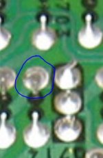
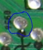
Your board needs to be resoldered first. You can do it selectively or resolder the whole board but beware not to made solder bridges. If u happen to make one, clear it then and there.
Look at the two attachments. These solders have a crack due to solder creep.
Gajanan Phadte
Look at the two attachments. These solders have a crack due to solder creep.
Gajanan Phadte
Attachments
Wooly, I'd heard about the fake components, and seen B&D mentioned in a thread either here or elsewhere as a reliable supplier of genuine parts, specifically in relation to these sony transistors. (the mains). It was only one individual though, so if anyone has any feedback on them, I'd definitely like to hear it.
Thanks for the links, I've been looking at the datasheets a bit, but I usually just punched it into google. That will definitely be a resource.
My recent searches pointed to suffixes being gains, and I poked around again in the datasheet, after a search for the suffix number turned up the same datasheet. So I looked a bit closer at the sheet, and it is indeed a gain designation/classification.
Both the 2SC2958 and 2SA1221 have a gain of 100-400 min/max. L=160-320 and K=200-400. The MJE pairs have a range of 30-240. Curves at 2v on the MJE's top out under 100, and the 2S's are just under 200. Would this be an issue?
I'll be sure to ask whenever I've got a question. Been learning a bunch on this project!
@gajanan: Thanks for pointing that out. I'd actually just re-checked another spot where a transistor has been heating things up for cracking, and found a couple more connections that need re-soldering. I'll have to look over the board carefully and at least re-solder all the questionable points.
The outright gain of the transistors shouldn't be an issue. It is the components around the transistors that determine the actual circuit performance to a very large extent. For example the voltage gain of the circuit (how much output for a given input) is determined by the ratio of resistors R711 and R712, not the transistor gains.
The MJE's should be universally available.
The MJE's should be universally available.
Gain at various levels
Hi Mooly. Sorry to bring this up, but I have one question regard gain in another part of a circuit.
The mentioned 2SA1221/2SC2958 (for example) are located in the circuit as drivers, right? Being drivers more "robust", they can handle much more current and are able to dissipate heat more than those which smaller packge, so hence the suggestion of MJE340/350, even if they have lower gain number.
But looking at differential input stage, however, the transistors, "by default", usually have much higher gain level, i.e. ~hFE 800 and higher, and especially in some vintage units where values of over hFE 1000 can be found. So, do the components around these transistors (differential) also determine the actual circuit performance to some extent? In case I have to deal with one of these transistors, I was just curious... Thanks.
The outright gain of the transistors shouldn't be an issue. It is the components around the transistors that determine the actual circuit performance to a very large extent. For example the voltage gain of the circuit (how much output for a given input) is determined by the ratio of resistors R711 and R712, not the transistor gains.
The MJE's should be universally available.
Hi Mooly. Sorry to bring this up, but I have one question regard gain in another part of a circuit.
The mentioned 2SA1221/2SC2958 (for example) are located in the circuit as drivers, right? Being drivers more "robust", they can handle much more current and are able to dissipate heat more than those which smaller packge, so hence the suggestion of MJE340/350, even if they have lower gain number.
But looking at differential input stage, however, the transistors, "by default", usually have much higher gain level, i.e. ~hFE 800 and higher, and especially in some vintage units where values of over hFE 1000 can be found. So, do the components around these transistors (differential) also determine the actual circuit performance to some extent? In case I have to deal with one of these transistors, I was just curious... Thanks.
At a very basic level you will find that fitting transistors with higher gain will allow the 'open loop gain' (that is gain with no feedback) to be higher than transistors of lower gain. That might translate to a gain of say 10000 vs 7000. When the feedback loop is closed the gain of the two is virtually identical, however because distortion is also reduced by the action feedback, the amp with higher open loop gain will end up with a slightly better distortion figure than than the lower one... but the effect is small.
For input devices there are other aspects to consider such as intrinsic junction capacitance and output capacitance but again, for small signal devices in typical audio applications the effect is small. If you tried using 2N3055's to make a differential front end then you would start to see the effects much more.
For input devices there are other aspects to consider such as intrinsic junction capacitance and output capacitance but again, for small signal devices in typical audio applications the effect is small. If you tried using 2N3055's to make a differential front end then you would start to see the effects much more.
Thank you, Mooly 🙂
I just ordered a bunch of KSA992's to replace an old 2SA798, but the BC560C's that I have here should do the job, too.
I just ordered a bunch of KSA992's to replace an old 2SA798, but the BC560C's that I have here should do the job, too.
- Status
- Not open for further replies.
- Home
- Amplifiers
- Solid State
- Sony STR-D315 Repair/troubleshooting