This chip is/was used in Cambridge CD2, CD3 and the DAC3 (I think) from my understanding the digital data signal goes into that then goes to the DAC chips.
My question is I repaired one that failed, it was the only real problem that needed addressing to get sound out. Why was it so simple? well it seems to be a very very common problem and my question today if anyone has any answers ias to why does it fail so often? Its a bit late to complain to the manufacturer since its 30 + years old but just very curious as to why those particular chips fail even before the caps!?
There seems to be not much information online and I wondered if there was a replacement but when I googled the replacement part nothing came up. Thanks!
I have no idea why it failed. Even though IC's are generally very stable, they can fail without any apparent external reason.
How many have you seen fail?
Regarding replacement, there seems to be plenty of options. A direct replacement could be:
https://www.ti.com/product/SN74LS166A
This can most likely also be used:
https://www.ti.com/product/CD74HCT166
Both are available in SO and DIL packages.
How many have you seen fail?
Regarding replacement, there seems to be plenty of options. A direct replacement could be:
https://www.ti.com/product/SN74LS166A
This can most likely also be used:
https://www.ti.com/product/CD74HCT166
Both are available in SO and DIL packages.
Why was it so simple?
Apparently, even a fault cannot please everyone.
It must have failed due to the years of heavy shifting.
Thanks for the information. I didn't know modern parts were available but I had no issue getting an old stock. This was a few years back now.
From the internet there's several people with the CD2 and CD3 that suffer from the same problem.
Would the modern parts be necessarily any better or just the design itself as suggested puts a heavy load on the chip causing it to fail too?
From the internet there's several people with the CD2 and CD3 that suffer from the same problem.
Would the modern parts be necessarily any better or just the design itself as suggested puts a heavy load on the chip causing it to fail too?
Digital logic chips can fail but simple ones like that I find strange. Would mostly be of overvoltage or an overcurrent somewhere.
In the all the Cambridge devices they go straight from the oversampling chip to SN chips then straight to the 4 TDA DACs.
In my particular case (CD2) a single 7805 regulator powers all ICs including the DACs.
The regulator had not failed. Neither had the caps. I would have thought it would be more under current than over. Obviously I can be completely wrong
In my particular case (CD2) a single 7805 regulator powers all ICs including the DACs.
The regulator had not failed. Neither had the caps. I would have thought it would be more under current than over. Obviously I can be completely wrong
Is it located close to something that becomes hot?
The IC itself seems to have a power consumption of around 150mW.
What kind of PCB is used (does it have a good or poor heat transfer)?
Over-voltage might be another reason. The LS devices have a fairly narrow supply window.
The HCT version has a wider supply window and of course a much lower power dissipation.
But there might be reasons why a CMOS part won't work in this application. Without a schematic and tests, it is difficult to say.
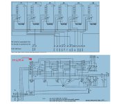
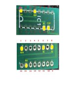
You can see from the photo attached its the PCB being the 4 vertical DAC boards. The schematic shows wheres it connected. Someone has drawn the schematic and I hope they dont mind me using it for studying purposes. As you can see all the main data lines to go it, get buffered? then output into the DACs, DAC1, 2 3, 4.
I didnt post a schematic of the PSU as its just one 7805 regulator. Also the picture is CD2 but the shematic is CD3. The PCB with the SN chips are identical but in the DAC3 according to a post most are SN but some are different. Its in Diyaudio if anyone wants me to find and share?
I didnt post a schematic of the PSU as its just one 7805 regulator. Also the picture is CD2 but the shematic is CD3. The PCB with the SN chips are identical but in the DAC3 according to a post most are SN but some are different. Its in Diyaudio if anyone wants me to find and share?
Attachments

The only oddity I see is the pre-emphasis relay coil has no diode. Maybe some voltage spike getting to the LS devices. As Jens mentions, LS is 5V and not very tolerant. Heat would be another, but the photo shows a layout that doesn't look bad for heat. Plenty of space. I've got LSTTL stuff I built in the 70's or 80's still working.


Only one capacitor for an entire board with shift registers, the board being a two-layer board without ground or supply planes? (At least that's what it looks like on the photo.)
In the days when 74LSxx ICs were used all over the place, there usually was a capacitor for each one of them. You might get away with less when you have a board with very low supply and ground inductance, like a four-layer board with a ground and a supply plane.
That is, the supply decoupling is rather poor, so there could be substantial ripples between supply and ground. The SN74LS166 can handle voltage peaks up to 7 V without damage, but its inputs only 5.5 V, according to the absolute maximum ratings in the datasheet.
It was common practice to tie off 74LS inputs that need to be high via a 1 kohm resistor to the supply, rather than directly. The resistor limited the current flowing into the input during a voltage peak, making the circuit less vulnerable. However, the SH/not LD inputs are all tied straight to the +5 V, according to the schematic you posted.
A 74HCT166 won't work without board modifications, because many other inputs that have to be high are left floating. It's particularly the not CLR input that would need to be tied high when you use 74HCT166. For 74HCT, tying high can be done with a wire straight to the +5 V, there is no need for a 1 kohm resistor (although it would not do any harm either).
A floating input is interpreted as high by 74LS logic, albeit with less noise margin than when it is tied off with a 1 kohm resistor to the +5 V. (Leaving inputs floating was therefore not recommended.) For 74HCT logic, an open input is undefined: depending on leakage currents, it can float high, low, high on a rainy day and low otherwise... Besides, you can get extra supply current due to floating inputs.
Last edited:
Not sure about 74166, but I've operated 7404 and 7473 (LS types) at 10V by mistake and they worked well. However, it may have stressed them so much that a substantial amount of their useful lifetime must have been consumed in the process.
TTL or CMOS, do not float unused inputs, always return them to GND or Vcc, preferably through a resistor.
TTL or CMOS, do not float unused inputs, always return them to GND or Vcc, preferably through a resistor.
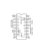
I tried reading your explanations several times and I'm struggling to understand. So I have very carefully copied the exact pinouts of the chip and marked it to hopefully answer some questions in order to help me understand easier.
Please note there are 0 resistors on the board itself might be some off the board but certainly not on the board itself. There is only one decoupling cap. And its seems the pin 15 and 16 are going straight to 5v.
Clearly it was minimal design and perhaps kept this way for best performance/less noise but more prone to damage?
This technology was so far ahead that Cambridge scrubbed off the writing on the chips to hide their secret as the CD players had an incredible smooth sound that some have pointed out would have not been possible without these chips doing stuff to the data lines first.
It has been suggested to tie the unsued inputs down with a resistor?
Love all the input!! 👍
Attachments
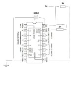
If I were to fix it, I would replace the damaged SN74LS166N with a new SN74LS166N or SN74LS166AN but with pin 15 bended such that it makes no contact with the PCB, see if I could somehow disconnect pins 15 of the other SN74LS166Ns, add small 1 kohm resistors between pins 15 and the +5 V, add 1 kohm resistors between pins 9 and the +5 V, leave inputs A...H as is and add a decoupling capacitor between pin 16 and pin 8 of each 74LS166. If it's more practical, you can use a common 1 kohm resistor for several inputs.
I might even do a small new board with the same footprint for the edge connector and any board supports and add in some more bypass caps as well as tieing off unused inputs with R's. if space is tight, use smd R's. Looks like plenty of space though. New board would likely not cost much more than the new replacement chips. new board could have a full ground plane as well since I think the original is single sided.
It has been suggested to tie the unsued inputs down with a resistor?
In the 74LS databooks, 1 kohm to +5 V was the usual recommendation for inputs that were to be tied high. Inputs that had to be tied low (in this case pin 6, clock inhibit) could be connected straight to ground.
OK from my understanding this is what I got so far. In orignal board the CLR pin 9 was left floating. In this case its tied with 1k to 5v.
Also all the inputs are left floating and not used A-H in original. I noted it was mentioned noise may be introduced if it was connected via 1k to 5v. So is there a need?
My original question was why does this fail? So far from my basic understanding of this chip, the relay may have had some affect, although it was a pre-emphasis and I guess only switched on when certain CD's were used.
And the other cause may have been from the pin 15 not having a resistor?!?
Lets just assume the pre-emphasis relay was taken out. With the design now given in the drawing attached would this be performing optimally and free from circuit design failure?
Another question just came to mind, would I use 1k for pin 15 and pin 9 per chip or would I tie all pin 15 to one 1k. What about pin 9? Each 1k or just one for all 6 chips? Note pin 9 was left floating before.
Thanks for the input!!
Attachments
Also all the inputs are left floating and not used A-H in original. I noted it was mentioned noise may be introduced if it was connected via 1k to 5v. So is there a need?
That's not quite what I meant. Noise margin is jargon for the difference between a high or low level and the switching threshold of a digital circuit.
When you leave 74LS inputs open, they are seen as high, but it's a bit wonky. With some crosstalk from other digital signals, they might occasionally be seen as low.
For inputs A...H, this doesn't matter, as the levels on these inputs are never used in your circuit anyway. Connecting A...H to the supply via 1 kohm would do no harm, but no good either. (This is all assuming you stick to 74LS logic, it's different for 74HCT.)
Pins 9 and 15 should be tied to the supply via 1 kohm resistors. Tied high to ensure they are always seen as high and via resistors to make the circuit more robust against supply voltage peaks.
You can use a common resistor for several inputs. In theory up to 100 inputs, but I wouldn't go above a dozen or so.
And the other cause may have been from the pin 15 not having a resistor?!?
That combined with poor supply decoupling, yes. Of course it's only a hypothesis.
- Home
- Source & Line
- Digital Line Level
- SN74LS166N shift chip why does it fail?