Alrighty then.
I've had a few channels of these built over the years and I always assumed that Slone's PCB would be good enough to realise the performance of the amp.
WRONG!
I was surprised to find, that upon measuring (I hadn't done this before as I'd assumed the PCBs to be up to the task.) that the distortion was wildly over the top.
0.015% THD (wow high -.-) @ 1khz into an 8 ohm load was typical and remained roughly at this level all the way up until clipping. I could lower the distortion down to ~0.005% by biasing the amp into Class A, which definitely hinted at things being amiss.
I found this website of Self's which promptly resulted in me buying his book. I have to say I like this book.
Anyway after playing about with some ill-conceived ideas in a simulator I decided to redesign the PCB for the 11.4, based upon reading what Self had said.
Simulation indicates that this amp should easily fall within the category that Self likes to call 'blameless' and I'm wondering how likely it is that you can actually achieve the measured performance indicated in Self's good book.
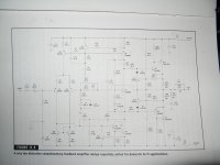
Here's a picture of the PCB. As much surface mount as I wanted to get away with - I hate drilling holes. (The image is rather large at just over 600k)

The blue arrow on the right shows the NFB take off point, the blue arrow on the left showing where it enters the input stage. The trace from the far right basically runs down the middle of the PCB.
The yellow arrows show where the various grounds for the signal ground are. The input filter, the cap and diode points on the NFB connection and the ground of the CCS. Red shows the ground of the VAS.
There is simply a large lump of copper on the bottom that connects all these together.
The large caps to the left of, and at the top and bottom of the driver/bias transistor heatsinks, are the bypass caps. These also have, to their left, a 0.1uf smd cap in parallel with them.
Again there is a thick track of copper running from the top to the bottom joining the ground connection from these together.
Initially I had the VAS transistor attached to the signal ground, then I tried connecting it to the power ground, which didn't really make any difference.
As you can see a shielded cable connects to the signal input and signal ground. A wire then goes from the signal ground directly to the signal ground star point.
A separate wire goes from the power ground back to a different point just after the PSU smoothing caps.
I've got the ground of the output connected directly back to the signal ground star point too.
The zobel I wasn't entirely sure where to connect so I soldered it directly to the output terminal.
The power leads are tightly twisted together and solder in, on the bottom, separately at the fuses. I initially had them soldered in on the top, moving them to the bottom didn't do much though.
More in a moment.
I've had a few channels of these built over the years and I always assumed that Slone's PCB would be good enough to realise the performance of the amp.
WRONG!
I was surprised to find, that upon measuring (I hadn't done this before as I'd assumed the PCBs to be up to the task.) that the distortion was wildly over the top.
0.015% THD (wow high -.-) @ 1khz into an 8 ohm load was typical and remained roughly at this level all the way up until clipping. I could lower the distortion down to ~0.005% by biasing the amp into Class A, which definitely hinted at things being amiss.
I found this website of Self's which promptly resulted in me buying his book. I have to say I like this book.
Anyway after playing about with some ill-conceived ideas in a simulator I decided to redesign the PCB for the 11.4, based upon reading what Self had said.
Simulation indicates that this amp should easily fall within the category that Self likes to call 'blameless' and I'm wondering how likely it is that you can actually achieve the measured performance indicated in Self's good book.
Here's a picture of the PCB. As much surface mount as I wanted to get away with - I hate drilling holes. (The image is rather large at just over 600k)
The blue arrow on the right shows the NFB take off point, the blue arrow on the left showing where it enters the input stage. The trace from the far right basically runs down the middle of the PCB.
The yellow arrows show where the various grounds for the signal ground are. The input filter, the cap and diode points on the NFB connection and the ground of the CCS. Red shows the ground of the VAS.
There is simply a large lump of copper on the bottom that connects all these together.
The large caps to the left of, and at the top and bottom of the driver/bias transistor heatsinks, are the bypass caps. These also have, to their left, a 0.1uf smd cap in parallel with them.
Again there is a thick track of copper running from the top to the bottom joining the ground connection from these together.
Initially I had the VAS transistor attached to the signal ground, then I tried connecting it to the power ground, which didn't really make any difference.
As you can see a shielded cable connects to the signal input and signal ground. A wire then goes from the signal ground directly to the signal ground star point.
A separate wire goes from the power ground back to a different point just after the PSU smoothing caps.
I've got the ground of the output connected directly back to the signal ground star point too.
The zobel I wasn't entirely sure where to connect so I soldered it directly to the output terminal.
The power leads are tightly twisted together and solder in, on the bottom, separately at the fuses. I initially had them soldered in on the top, moving them to the bottom didn't do much though.
More in a moment.
how do I download the image?
I would like to say "ignore Slone, he has nothing useful to say" but I have not read his book, so it would be presumptuous to assume all his publications are as bad as the few topics (he gets wrong) that get discussed on this Forum.
I would like to say "ignore Slone, he has nothing useful to say" but I have not read his book, so it would be presumptuous to assume all his publications are as bad as the few topics (he gets wrong) that get discussed on this Forum.
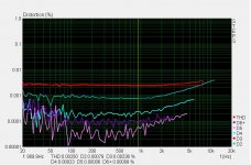
Now to the measured performance (and where my problems begin.)
First a measurement of the system that will be used for measurements. Taken at 96khz.

This varies with the time of day. It's usually better late at night when people have gone to bed - less electrical noise floating around? Perhaps.
Next is a measurement taken at 8 volts p-p into my 9.4ohm test load.

First of all you can see that the second harmonic is actually lower here then in the actual measurement of the 'soundcard'. This is a dual mono implementation of the PCM1794 DAC + PCM4202 ADC. And it shows how the performance varies with time as the first measurement was taken on a different day.
The overall distortion here is reasonably low and should be pretty much entirely off the audible radar.
Now the fun begins.
I'm going to link a series of measurements. These are all taken whilst driving my 9.4 ohm dummy load. There will be two sets of graphs, taken in pairs at 1khz and 10khz. These are at drive levels of 13 volts and 70 volts p-p (just before clipping).
1khz 13v

10khz 13v

1khz 70v

10khz 70v

Performance like that is quite respectable you might say, but I find it a little perplexing. What isn't shown is a third set of data I took at around 26 volts p-p. Distortion remains roughly the same up until that point, then starts to degrade as drive level is increased.
The most confusing part is this next graph...

This is once again taken at 70volts p-p, but this time with no load attached. And this is where I scratch my head.
The distortion at 1khz = the same whether or not the 9.4ohm load is attached to it or not.
Now it is my understanding that the 1khz distortion should remain pretty much ~0.0005% up until around clipping, with no load. Then it should measure considerably worse with the load attached.
This also leads me to believe that I am not being troubled by distortion 5 or 6 in Self's book ( Bad rail decoupling and Induction distortion) because these are entirely dependant on their being half wave sine pulses on the power lines. With no load attached there's zero pulses as the amp isn't having to deliver any current. I've measured this and indeed very low ripple and zero sine pulses.
Biasing the amplifier into Class A also doesn't solve these problems (as you'd expect), it can give slightly lower figures in certain places at certain drive levels, but this is to be expected also. This also leads me to believe that the point I've taken the feedback off isn't to blame either - although I'm open to suggestions on that part.
I have most certainly used NPO/COG caps in the feedback circuit and also in the 2pole comp circuit. I'd be surprised if they were suspect, but again that's open to consideration.
Now, the wire that carries the output from the board to the terminal on the case.
I can degrade the distortion performance by moving this around, but only at high frequencies and if there's a load present. This isn't really surprising and moving the wire around at 1khz doesn't really affect much.
This is the time where you turn around say, welcome to the real world. Yes I am aware that the overall THD I'm getting is better or equal to the vast majority of consumer amps I have seen measured. However reading Self's book leads you to believe that maintaining ~0.000x distortion figures for 1khz, before clipping, should be achievable.
Am I crazy in thinking that? I'm certainly not disappointed with the results, but I have a feeling I might be able to do better.
First a measurement of the system that will be used for measurements. Taken at 96khz.
This varies with the time of day. It's usually better late at night when people have gone to bed - less electrical noise floating around? Perhaps.
Next is a measurement taken at 8 volts p-p into my 9.4ohm test load.
First of all you can see that the second harmonic is actually lower here then in the actual measurement of the 'soundcard'. This is a dual mono implementation of the PCM1794 DAC + PCM4202 ADC. And it shows how the performance varies with time as the first measurement was taken on a different day.
The overall distortion here is reasonably low and should be pretty much entirely off the audible radar.
Now the fun begins.
I'm going to link a series of measurements. These are all taken whilst driving my 9.4 ohm dummy load. There will be two sets of graphs, taken in pairs at 1khz and 10khz. These are at drive levels of 13 volts and 70 volts p-p (just before clipping).
1khz 13v
10khz 13v
1khz 70v
10khz 70v
Performance like that is quite respectable you might say, but I find it a little perplexing. What isn't shown is a third set of data I took at around 26 volts p-p. Distortion remains roughly the same up until that point, then starts to degrade as drive level is increased.
The most confusing part is this next graph...
This is once again taken at 70volts p-p, but this time with no load attached. And this is where I scratch my head.
The distortion at 1khz = the same whether or not the 9.4ohm load is attached to it or not.
Now it is my understanding that the 1khz distortion should remain pretty much ~0.0005% up until around clipping, with no load. Then it should measure considerably worse with the load attached.
This also leads me to believe that I am not being troubled by distortion 5 or 6 in Self's book ( Bad rail decoupling and Induction distortion) because these are entirely dependant on their being half wave sine pulses on the power lines. With no load attached there's zero pulses as the amp isn't having to deliver any current. I've measured this and indeed very low ripple and zero sine pulses.
Biasing the amplifier into Class A also doesn't solve these problems (as you'd expect), it can give slightly lower figures in certain places at certain drive levels, but this is to be expected also. This also leads me to believe that the point I've taken the feedback off isn't to blame either - although I'm open to suggestions on that part.
I have most certainly used NPO/COG caps in the feedback circuit and also in the 2pole comp circuit. I'd be surprised if they were suspect, but again that's open to consideration.
Now, the wire that carries the output from the board to the terminal on the case.
I can degrade the distortion performance by moving this around, but only at high frequencies and if there's a load present. This isn't really surprising and moving the wire around at 1khz doesn't really affect much.
This is the time where you turn around say, welcome to the real world. Yes I am aware that the overall THD I'm getting is better or equal to the vast majority of consumer amps I have seen measured. However reading Self's book leads you to believe that maintaining ~0.000x distortion figures for 1khz, before clipping, should be achievable.
Am I crazy in thinking that? I'm certainly not disappointed with the results, but I have a feeling I might be able to do better.
how do I download the image?
I would like to say "ignore Slone, he has nothing useful to say" but I have not read his book, so it would be presumptuous to assume all his publications are as bad as the few topics (he gets wrong) that get discussed on this Forum.
>.< Cant you see the images? They show up fine for me, they are in my gallery.
I tried logging out and the picture in the first thread didn't appear. Are the images working in the second post?
Here's the first image again.

Here's the first image again.
this sounds suspicious.A separate wire goes from the power ground back to a different point just after the PSU smoothing caps.
I've got the ground of the output connected directly back to the signal ground star point too.
The zobel I wasn't entirely sure where to connect so I soldered it directly to the output terminal.
The ground near the smoothing caps is the main Audio Ground.
All the other grounds connect to here, provided the Audio ground has a single wire link back to the zero volts point between the smoothing caps.
The Zobel and the speaker and the PCB power all connect to the main Audio Ground.
The Signal Ground can connect via it's own wire to the Audio Ground. This may be from the RCA socket or from the PCB signal ground pad.
If this gives hum then consider adding a 10//diode//inverse diode into the Signal Ground to Audio Ground link wire.
The Zobel is part of the Thiele Network that helps stabilise the amp by providing a high frequency load.
My views on this have changed.
The first R+C (Zobel part) should be very close to the amp output. preferably designed into the PCB to minimise inductance in the connection from output transistors to PCB power ground.
The second R//L should be off PCB and used as part of the route to the chassis output terminal.
The third part is usually missed out, but I have started using an R+C across the chassis speaker terminals. Again keeping it all optimised to minimise inductance on the route between the terminals.
This three part Thiele network is Pi filter and provides a very consistent load for the amp at VHF and also helps isolate cable and speaker impedances from the amplifier. It further acts as an effective HF filter attenuating back emf and/or emi to the NFB input point.
this sounds suspicious.
The ground near the smoothing caps is the main Audio Ground.
All the other grounds connect to here, provided the Audio ground has a single wire link back to the zero volts point between the smoothing caps.
The Zobel and the speaker and the PCB power all connect to the main Audio Ground.
This isn't what Self says. He says that Rail decoupler capacitors - which are the only things that actually have power ground in this amplifier, as far as I know - must have a separate ground return to the reservoir ground. This must not share any part of the audio ground system, and must not be returned to the star-point.
Are you implying that I ignore this and connect the power ground directly to the star point?
I'm going to try re-grounding the zobel and see what happens.
no, Self is right..... Rail decoupler capacitors .............. must have a separate ground return to the reservoir ground. This must not share any part of the audio ground system, and must not be returned to the star-point.
Are you implying that I ignore this and connect the power ground directly to the star point?
Look at his diagrams. His star point and your "ground" are not the same.
His diagram explains.
The small caps look NP0/C0G-ish to me. What is their voltage rating?
Can you try foil caps in their place just to rule out the possibility of them beeing a problem?
Is that a CFP output stage? (just curious if I spottet that correctly)
Can you try foil caps in their place just to rule out the possibility of them beeing a problem?
Is that a CFP output stage? (just curious if I spottet that correctly)
Altering the layout of the grounding didn't really solve much. In fact it didn't change anything, that includes altering the return for the power ground.
This doesn't seem to be ground/PSU/induction related, or I'd expect the distortion to change dramatically depending on the load the amp is driving. Am I wrong in assuming this?
Is this a problem at all? Currently I stop getting 0.000x distortion, turning into 0.00x at about 37 volts p-p into either the 9.4 or 4.7 ohm dummy loads at 1khz.
I'm also getting 115 watts into 4.7 ohms @ 1% THD @ 1khz and 85 watts into the 9.4 ohm load under the same conditions.
The 4.7 ohm test seems prematurely limited by the +ve protection. If they were symmetrical I'd be getting just under 135 watts into 4.7 ohms, although this is really academic. The only part of the system that's 4 ohms is the tweeter and the system is entirely active, I never use more then 1-2 watts for the tweeter.
The small caps look NP0/C0G-ish to me. What is their voltage rating?
Can you try foil caps in their place just to rule out the possibility of them beeing a problem?
Is that a CFP output stage? (just curious if I spottet that correctly)
The Zobel is a film cap already, a PEN type that I've used successfully in the past.
Yes they are all NPO/COG, the decouplers are rated at 100V.
The 150 and 330pf in the 2pole comp are rated at 1000 and 200 volts respectively. However! I have noticed that the 5pf (I used 4.7) used at the start of the feedback network is only rated at 50volts DC.
I made sure that they were all high voltage devices, but it appears the reason I ordered a 50v device was because it was the only one they had in that case style.
In simulation that cap has the full output voltage across it. Now I thought caps had a higher voltage rating for AC over DC. Either way, do you think that could be the cause? The amp starts to show rising distortion at around 25v p-p. I suppose that could be cap non-linearity .
Edit - yes its CFP.
no, Self is right.
Look at his diagrams. His star point and your "ground" are not the same.
His diagram explains.
I have a really thick trace of copper on a PCB that the reservoir caps connect to. At one end of this I've got the output relay ground return, I also had the return for the decoupling caps attached here.
Off this large copper trace I've taken one wire a short distance (2cm) to which I have soldered a tiny bit of unetched PCB, this I am using as the signal star ground.
In Self's book he's got the input cable ground soldered to the input connector, as have I. The other end of the input cables ground then connects to the feedback networks ground at a point, then this point is taken to the signal star ground.
I have the feedback ground merging with the other end of the input cable ground on the PCB. This is taken via a wire to the signal star ground.
Self has the return path for the output connected directly to the signal star ground, as have I.
The only difference is that he shows the decoupling caps attached to a point further 'on' as it were from the signal star point, rather then closer to the reservoir caps. I couldn't understand why you would want the return feed, that was potentially dirty flowing by the signal ground. Unless I misinterpreted the diagram, so I connected the decoupling caps at the end of the reservoir caps pcb trace - I have tried moving this elsewhere to no effect.
If I am not understand something here please elaborate.
If the voltage across this cap in the feedback network really rises to reasonably high values in the order of its voltage rating at audio frequencies, it is possible that this results in a raised THD.
<But this ought to show a rising slope towards high frequencies, as the voltage across the device increases.> wrong
<So this cap could not explain a raised THD that is constant over frequency.> wrong
EDIT:
Sorry, the last sentence is of course completely wrong.
The voltage across the cap is constant at audio (low) frequencies and then falls with frequency. And this would perfectly explain a constantly raised THD over frequency, if any distortion is introduced by the cap.
Last edited:
If possible, then please post the first image once again
The schematic image i hope.
regards,
Carlos
The schematic image i hope.
regards,
Carlos
The schematic image i hope.
regards,
Carlos
The grounding scheme is in Self's book if that is to what you are requesting.
As for the amp, forgive the lo-tech approach!
Attachments
If the voltage across this cap in the feedback network really rises to reasonably high values in the order of its voltage rating at audio frequencies, it is possible that this results in a raised THD.
<But this ought to show a rising slope towards high frequencies, as the voltage across the device increases.> wrong
<So this cap could not explain a raised THD that is constant over frequency.> wrong
EDIT:
Sorry, the last sentence is of course completely wrong.
The voltage across the cap is constant at audio (low) frequencies and then falls with frequency. And this would perfectly explain a constantly raised THD over frequency, if any distortion is introduced by the cap.
Yes actually this does and its almost entirely third order.
When I've made STEPS measurements at high power levels, all the harmonics are acceptably low, except third which remains constant in level and unreaslitically high.
So say third harmonic would be 0.002% from 20hz to 2khz, the rest being 0.000x. Then as frequency rises distortion also rises as you'd expect.
This would also explain why its independent of load too as the voltage impressed across the cap doesn't change, if anything it gets lower under PSU droop.
This 3rd harmonic really looks suspicious in "favour" of C6.
If possible (still stable) i would take it out and see what happens to the 3rd harmonic plot.
If possible (still stable) i would take it out and see what happens to the 3rd harmonic plot.
- Status
- Not open for further replies.
- Home
- Amplifiers
- Solid State
- Slones 11.4 'Blameless'