Hello, can someone tell me how good is this schematic. Are there any willing folks, that are good with the simulating programs to make me a virtual test.
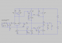
Reason being - I have two pcb's almost assembled for a hearing test, but I'm not sure if the constant current source for the VAS is correctly calculated. And how low can the miller cap be reduced to improve the sonics, but without a risk of oscillation. Also - why did uncle Rod put a miller cap in the negative rail driver ? And can we reduce/remove that also? 🙂
This is the schematic. 🙂
p.s. When simulating /if someone ever does/ it would be good to put some test voltages in appropriate spots of the schematic for troubleshooting. Just in case. 🙂
Reason being - I have two pcb's almost assembled for a hearing test, but I'm not sure if the constant current source for the VAS is correctly calculated. And how low can the miller cap be reduced to improve the sonics, but without a risk of oscillation. Also - why did uncle Rod put a miller cap in the negative rail driver ? And can we reduce/remove that also? 🙂
This is the schematic. 🙂
An externally hosted image should be here but it was not working when we last tested it.
p.s. When simulating /if someone ever does/ it would be good to put some test voltages in appropriate spots of the schematic for troubleshooting. Just in case. 🙂
Last edited:
I did some quick simulations. If the voltage drop over the LED is 2.5 V then the VAS CCS quiescent current is 18.3 mA and the LTP CCS quiescent current is 3.39 mA.
When VR1 is set to 2k2 the output quiescent current is ~700 mA!
When VR1 is set to 0R1 the output quiescent current is ~24.5 A!
I'm attaching the LT Spice .asc schematic file and an image of it.
I might do some more simulations tomorrow to find better values for
R16, VR1 and R9 to lower the output quiescent current which is way to high now.
Attachments
Actually, I forgot to mention it in my circuit drawing program - the led is a diffused green one, advertised forward drop is 1.7V.
From that point on, I think both quiescent currents of the CCS's will be lower, and the output quiescent also. 🙂
I did the theory /circuit/ of this hybrid a while ago /year or so/, but still didn't get a chance to test it /in reality, heck even in virtuality/.
If I remember correctly with the diffused green led my calculations about the VAS were about 7mA or so, and about 1-2mA for the LTP. 🙂
Overall ... is it holding on? No strange things happening? The main point of these gymnastics was to add a little more linearity to the input and VAS stages and minimize the DC offset. And still remain the fair simplicity of the cult called P3A.
Last edited:
Hi K,
Maybe give the CC sources their own bias - I tried this before with poor results.
With the current mirror added you should consider emitter resistors in the LTP.
The vbe multiplier might need some work (as mentioned already).
Maybe give the CC sources their own bias - I tried this before with poor results.
With the current mirror added you should consider emitter resistors in the LTP.
The vbe multiplier might need some work (as mentioned already).
1.7 V drop over the LED gives the following from the sim:
LTP CCS: 1.88 mA
VAS CCS: 11.27 mA
OPS Iq @ VR1=0R1: 15.1 A
OPS Iq @ VR1=2k2: 628 mA
Still a bit high.
LTP CCS: 1.88 mA
VAS CCS: 11.27 mA
OPS Iq @ VR1=0R1: 15.1 A
OPS Iq @ VR1=2k2: 628 mA
Still a bit high.
Put a 1K resistor in the base of Q12, or give it its own reference, otherwise during clipping Q12 will pull the reference voltage down and affect the current source feeding the LTP. Also degenrate the LTP with 100 ohm resistors.
Personally I gave up when the CFP pair annoyed me too much.
Personally I gave up when the CFP pair annoyed me too much.
Today I was going trough the boxes that are on top of my wardrobe, and I found my test boards ... assembled! 😱
My brain sucks BIG time! LOL 😀 I don't seem to recall when did I finish them, so anyhow...modifications are down to the bare minimum, needed not to fry the circuit. The linearity will be in the next revision of the pcb, beacause space is something I don't have, and everything is very tight. I'll post up an updated schematic later with your suggestions. 🙂
jaycee ... what's wrong with the CFP ? In my opinion it's the best thing - practically indestructible. I was running the original P3A with +/-42V rails and 4ohm load on a pretty small heatsink, when my fan stalled and I didn't even notice, for TWO hours was I pumping the **** out of that amp, and it didn't fail, without any thermal tracking for the bias. When I plugged it off, my skin could easily stick on the heatsink if I touched it. 🙂
p.s. And my output devices weren't the best things - 2SC3281/2SA1302, but from the turkish-chinise type ***** with a 1.5x1.5mm die, beacause toshiba stopped making them before a long time ago.
Last edited:
My internet at home is dead right now, so I can't post any schematics. I have a question, thou - what will be the benefits /if there are any at all/ if we change the LTP with fets, like 2SK301 or so? Also I'm thinking of changing the CCS for the LTP with a dual-transistor type. /not sure how is the term in english/
And one last thing - my boards are assembled, and as I said - space is tight, my question is how can we correct the schematic to make it run as it is, and adjust like 60-100mA bias for the outputs, WITHOUT touching the trimmer - only R9/R16? 😕 The main goal is just to make them run, without frying anything, then I'll give these boards to a friend of mine, and we can start the evaluation of the circuit and board. When we're done with that, the final revision of the boards will be contribute to my ears. 😀
p.s. What will happen, if I power the circuit without the LTP emitter resistors, bare in mind that Q1-Q2 and Q10-Q11 are very closely beta-matched. I chose them myself. 😀
Last edited:
kalmara,
Very good idea. You should do that at once. Don´t use source resistors.we change the LTP with fets, like 2SK301 or so? Also I'm thinking of changing the CCS for the LTP with a dual-transistor type.
kalmara;
sorry, clarification is needed .
2SK301 will be fine with source resistors.
The output CFP could be problematic. Look out for oscillation. I would use MOSFETs for Q7/Q8.
sorry, clarification is needed .
2SK301 will be fine with source resistors.
The output CFP could be problematic. Look out for oscillation. I would use MOSFETs for Q7/Q8.
Any suggestions for *more-linear* easy accessible FET's for the input, besides 2SK301? 😀
Also - I want to stick with the CFP, because the lack of thermal tracking, and because I have a very small stack of original Toshiba devices /2SC5198-2SA1941/.
AFAIK the lateral mosfets are also self-biasing of some sort, but they are very expencsive, and I can't find original ones here in my town.
p.s. Lumba - about the source/emitter resistors, I won't use them in the first version of the amp - the one, that I have assembled. When I continue on with the PCB design, I'll make it a little bigger and fit everything in there. 😀
p.p.s About the quiescent currents in the first circuit - how about increasing R9 to 220ohm, to lower a bit the VAS CCS current, and decreasing R16 to like 560ohm, to lower the bias for the outputs when the VR is at maximum rating? /I'm not sure about the Vbe multiplier thou - should we increase or decrease the B-C resistor in order to lower the Vdrop?/
kalmara,
first of all, you need to make an important decision. Bipolar output devices won`t work flawlessly in this configuration. What about IRFP240/9240?
first of all, you need to make an important decision. Bipolar output devices won`t work flawlessly in this configuration. What about IRFP240/9240?
What about IRFP240/9240?
Same deal ... cheap and weak turkish/chinese garbage. 🙁
In wich configuration exactly do you think that the BJT's wont work *flawlessly*?
kalmara.
in class AB CFP. With BJTs, you should choose another output configuration or use MOSFETs.
in class AB CFP. With BJTs, you should choose another output configuration or use MOSFETs.
danfo098, which program are you using for the simulations? I found an old version ov Multisim at home /v7.0/ and layed out the circuit with a lot of effort, using 220ohms for R9, and the VAS CCS bias is about 5-6-7mA or so, I don't remember. Also the Vbe multiplier with its current state does pretty well when changing the variable resistor. I could easily adjust my bias to ~100mA and do a test with 1.3V sine at 1khz /the amp's a bit tripped considering input sensitivity/ that gave me my full output with no clipping and about 104W at 4ohms and +/-35V supply.
I'm using LT spice. The simulator is free and you can download it here:
Linear Technology - Design Simulation and Device Models
You might have to add models for the transistors though.
One thing that comes to mind now is that I'm using the BD139/140 spice models from ON Semiconductor and people on this forum say that those models are bad. They also say that the fairchild models are better, problem is they don't have their models available on their website so you have to request them and they might not answer.
The fairchild models might be available on this forum if you search though.
If you download LT spice you can use the .asc file I attached earlier. To add your own models look in the file /lib/cmp/standard.bjt in the LT spice directory. Just append more models at the bottom of the file.
The models I used in the simulation:
.model 2SA1302 PNP( IS=21.479E-12 BF=136.48 VAF=100 IKF=19.980 ISE=21.504E-12
+NE=1.3784 BR=329.48 VAR=100 IKR=19.980 ISC=4.3670E-9 NC=1.4264 RC=93.301E-3
+CJE=755.31E-12 MJE=.33333 CJC=1.1417E-9 MJC=.33333 TF=1.2802E-9 XTF=10 VTF=10
+ITF=1 TR=10.000E-9)
.model 2SC3281 NPN(IS=10.000E-15 BF=155.65 VAF=100 IKF=9.2028 XTB=1.5
+ISE=54.325E-15 NE=1.3056 BR=10.787 VAR=100 IKR=1.8561 ISC=106.69E-15
+NC=1.6728 RC=26.745E-3 CJE=2.0000E-12 CJC=534.41E-12
+MJC=.33333 TF=8.0821E-9 XTF=3.1968 VTF=21.461E-3 ITF=169.59 TR=187.91E-9 )
.model BD139 NPN( IS=1e-09 BF=222.664 NF=0.85 VAF=36.4079 IKF=0.166126 ISE=5.03418e-09 NE=1.45313 BR=1.35467 NR=1.33751 VAR=142.931 IKR=1.66126 ISC=5.02557e-09 NC=3.10227 RB=26.9143 IRB=0.1 RBM=0.1 RE=0.000472454 RC=1.04109 XTB=0.727762 XTI=1.04311 EG=1.05 CJE=1e-11 VJE=0.75 MJE=0.33 TF=1e-09 XTF=1 VTF=10 ITF=0.01 CJC=1e-11 VJC=0.75 MJC=0.33 XCJC=0.9 FC=0.5 CJS=0 VJS=0.75 MJS=0.5 TR=1e-07 PTF=0 KF=0 AF=1 Vceo=80 Icrating=1500m mfg=ONSEMI)
.model BD140 PNP ( IS=1e-09 BF=650.842 NF=0.85 VAF=10 IKF=0.0950125 ISE=1e-08 NE=1.54571 BR=56.177 NR=1.5 VAR=2.11267 IKR=0.950125 ISC=1e-08 NC=3.58527 RB=41.7566 IRB=0.1 RBM=0.108893 RE=0.000347052 RC=1.32566 XTB=19.5239 XTI=1 EG=1.05 CJE=1e-11 VJE=0.75 MJE=0.33 TF=1e-09 XTF=1 VTF=10 ITF=0.01 CJC=1e-11 VJC=0.75 MJC=0.33 XCJC=0.9 FC=0.5 CJS=0 VJS=0.75 MJS=0.5 TR=1e-07 PTF=0 KF=0 AF=1 Vceo=80 Icrating=1500m mfg=ONSEMI)
The BC546B and BC556B came with LT spice.
* BD136/138/140 PNP EPITAXIAL SILICON TRANSISTOR
*------------------------------------------------------
* MEDIUM POWER LINEAR AND SWITCHING APPLICATIONS
* Based on BD140-16
* BVcbo: BD135 -45V / BD137 -60V / BD139 -80V
* BVceo: BD135 -45V / BD137 -60V / BD139 -80V
* BVebo: -5V
* Complement to BD135, BD137 and BD139 respectively
*------------------------------------------------------
.MODEL BD136_138_140 PNP (
+ IS =2.9537E-13
+ BF =201.4
+ NF =1.0
+ BR =23.765
+ NR =1.021
+ ISE =1.8002E-13
+ NE =1.5
+ ISC =7.0433E-12
+ NC =1.38
+ VAF =137.0
+ VAR =8.41
+ IKF =1.0993
+ IKR =0.10
+ RB =1.98
+ RBM =0.01
+ IRB =0.011
+ RE =0.1109
+ RC =0.01
+ CJE =2.1982E-10
+ VJE =0.7211
+ MJE =0.3685
+ FC =0.5
+ CJC =6.8291E-11
+ VJC =0.5499
+ MJC =0.3668
+ XCJC =0.5287
+ XTB =1.4883
+ EG =1.2343
+ XTI =3.0 )
*-------------------------------------------------------
* FAIRCHILD CASE: TO-126 PID:BD140-16
* 2000-03-20 CREATION
* BD135/137/139 NPN EPITAXIAL SILICON TRANSISTOR
*------------------------------------------------------
* MEDIUM POWER LINEAR AND SWITCHING APPLICATIONS
* Based on BD135-16
* BVcbo: BD135 45V / BD137 60V / BD139 80V
* BVceo: BD135 45V / BD137 60V / BD139 80V
* BVebo: 5V
* Complement to BD136, BD138 and BD140 respectively
*------------------------------------------------------
.MODEL BD135_137_139 NPN (
+ IS =2.3985E-13
+ BF =244.9
+ NF =1.0
+ BR =78.11
+ NR =1.007
+ ISE =1.0471E-14
+ NE =1.2
+ ISC =1.9314E-11
+ NC =1.45
+ VAF =98.5
+ VAR =7.46
+ IKF =1.1863
+ IKR =0.1445
+ RB =2.14
+ RBM =0.001
+ IRB =0.031
+ RE =0.0832
+ RC =0.01
+ CJE =2.92702E-10
+ VJE =0.67412
+ MJE =0.3300
+ FC =0.5
+ CJC =4.8831E-11
+ VJC =0.5258
+ MJC =0.3928
+ XCJC =0.5287
+ XTB =1.1398
+ EG =1.2105
+ XTI =3.0 )
*-------------------------------------------------------
* FAIRCHILD CASE: TO-126 PID:BD135-16
* 2000-03-20 CREATION
*------------------------------------------------------
* MEDIUM POWER LINEAR AND SWITCHING APPLICATIONS
* Based on BD140-16
* BVcbo: BD135 -45V / BD137 -60V / BD139 -80V
* BVceo: BD135 -45V / BD137 -60V / BD139 -80V
* BVebo: -5V
* Complement to BD135, BD137 and BD139 respectively
*------------------------------------------------------
.MODEL BD136_138_140 PNP (
+ IS =2.9537E-13
+ BF =201.4
+ NF =1.0
+ BR =23.765
+ NR =1.021
+ ISE =1.8002E-13
+ NE =1.5
+ ISC =7.0433E-12
+ NC =1.38
+ VAF =137.0
+ VAR =8.41
+ IKF =1.0993
+ IKR =0.10
+ RB =1.98
+ RBM =0.01
+ IRB =0.011
+ RE =0.1109
+ RC =0.01
+ CJE =2.1982E-10
+ VJE =0.7211
+ MJE =0.3685
+ FC =0.5
+ CJC =6.8291E-11
+ VJC =0.5499
+ MJC =0.3668
+ XCJC =0.5287
+ XTB =1.4883
+ EG =1.2343
+ XTI =3.0 )
*-------------------------------------------------------
* FAIRCHILD CASE: TO-126 PID:BD140-16
* 2000-03-20 CREATION
* BD135/137/139 NPN EPITAXIAL SILICON TRANSISTOR
*------------------------------------------------------
* MEDIUM POWER LINEAR AND SWITCHING APPLICATIONS
* Based on BD135-16
* BVcbo: BD135 45V / BD137 60V / BD139 80V
* BVceo: BD135 45V / BD137 60V / BD139 80V
* BVebo: 5V
* Complement to BD136, BD138 and BD140 respectively
*------------------------------------------------------
.MODEL BD135_137_139 NPN (
+ IS =2.3985E-13
+ BF =244.9
+ NF =1.0
+ BR =78.11
+ NR =1.007
+ ISE =1.0471E-14
+ NE =1.2
+ ISC =1.9314E-11
+ NC =1.45
+ VAF =98.5
+ VAR =7.46
+ IKF =1.1863
+ IKR =0.1445
+ RB =2.14
+ RBM =0.001
+ IRB =0.031
+ RE =0.0832
+ RC =0.01
+ CJE =2.92702E-10
+ VJE =0.67412
+ MJE =0.3300
+ FC =0.5
+ CJC =4.8831E-11
+ VJC =0.5258
+ MJC =0.3928
+ XCJC =0.5287
+ XTB =1.1398
+ EG =1.2105
+ XTI =3.0 )
*-------------------------------------------------------
* FAIRCHILD CASE: TO-126 PID:BD135-16
* 2000-03-20 CREATION
Last edited:
- Status
- Not open for further replies.
- Home
- Amplifiers
- Solid State
- Slightly evolved P3A simulation