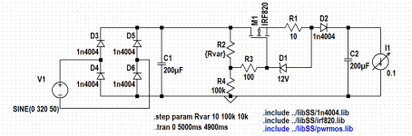
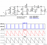
For a simple tube tester I'm planning to build, I want to regulate the screen voltage supply, so when testing pentodes I can change the voltage to get different measurements. Unregulated input will be 320 V DC with some ripple (perhaps 5%). I want to be able to go down to 60 V DC.
I want to develop my own circuit, instead of just copy some high performance design, thus I seek advice, because it is my first of these kind of circuits.
I'm looking to a simple approach, like a linear regulator based on a n-channel MOSFET like IRF820 or a beefer fqa11n90c (just .42ºC/W thermal resistance junction-case), and a voltage divider reference (so I can use a potentiometer to change the output voltage).
Attached, something I just simulated.
Is there anything bad with this?
Any tip from more experienced people?
I favor simple circuits which I can fully understand, to very complex and high performance solutions.
Just to give some more details, I guess I'll have to deal with a maximum of 100 mA of screen current during short intervals (<5ms), and an average of 50mA.
My transformer has two secondary high voltage taps, so choosing the top nearer one to my target voltage, I think that the maximum voltage drop in the regulator will be around 150 V maximum.
Just for those who don't know tubes, screen current is low when screen voltage is low, so the maximum dissipation for the MOSFET will be when using the higher voltage tap, around 5-10W peak, and lower average.
These are just very rough estimations.
Thank you for participating.
Attachments
A few comments:
In general it looks fine to me.
It may oscillate, so I would consider a capacitor between the gate and ground.
R1/D1 I assume to provide a kind of current limitation. Is the 10R value of R1 not too little with the output currents you mention? If R2 can go to zero, I guess D1 may have difficulties controlling the gate-voltage with R3 being only 100R. What about increasing R3?
Good points. Thank you.
Honestly, I chose 10R for the limiting resistor just because I've seen other similar circuits using that value (for similar current demands). The zener is to avoid the gate to be too high with respect to source.
I'll add a gate-ground capacitor. I just didn't consider stability, as I thought that it was of main concern with LDO topologies, not this classic regulator.
Why?If R2 can go to zero, I guess D1 may have difficulties controlling the gate-voltage with R3 being only 100R.
Honestly, I chose 10R for the limiting resistor just because I've seen other similar circuits using that value (for similar current demands). The zener is to avoid the gate to be too high with respect to source.
I'll add a gate-ground capacitor. I just didn't consider stability, as I thought that it was of main concern with LDO topologies, not this classic regulator.
Place a cap in there and you get lower noise output (cap multiplier function).
Also if you place an NPN over a 5ohm resistor you get current limiting to just over 100mA. Just an idea.
I dont like having controls like potentiometers at the high voltage rail, potential for high potential into fingers.
Also with the voltage span you are interested in the resistors and potentiometer (or stepped resistor) must be pretty big and heat sinked.
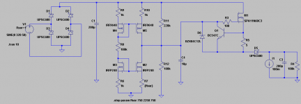
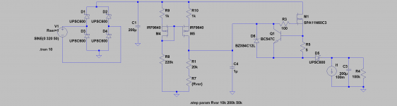
Heres one possible way of actively adjusting the voltage, but this requires 4 more MOSFETs so it may suddenly become complex...
Edit: The currentmirror MOSFETs used in the sim are not the ones of choice, but the ones I easy find in the sim lib. Do not use those at these voltages.
Also if you place an NPN over a 5ohm resistor you get current limiting to just over 100mA. Just an idea.
I dont like having controls like potentiometers at the high voltage rail, potential for high potential into fingers.
Also with the voltage span you are interested in the resistors and potentiometer (or stepped resistor) must be pretty big and heat sinked.
Heres one possible way of actively adjusting the voltage, but this requires 4 more MOSFETs so it may suddenly become complex...
Edit: The currentmirror MOSFETs used in the sim are not the ones of choice, but the ones I easy find in the sim lib. Do not use those at these voltages.
Attachments
Last edited:
Not really bad, but the output is not going to be regulated, in fact the opposite will happen: the regulation will be worse at the output than the input, and the ripple will not be attenuated.Is there anything bad with this?
Here is an example retaining most of the features of your initial circuit but avoiding most of its weaknesses.Any tip from more experienced people?
I favor simple circuits which I can fully understand, to very complex and high performance solutions.
It is also easy to understand and uses only ordinary components.
Just make sure the 100K pot has a plastic spindle.
The total adjustment range will be ~10:1, for example 25 to 250V.
Select R4 for something that suits you. D1 is an ordinary LED, red yellow or green; select it to compensate for the dispersion of the DN2540.
The output will be ripple-free and reasonably stable, with an output resistance of a few ohms.
Attachments
Also if you place an NPN over a 5ohm resistor you get current limiting to just over 100mA. Just an idea.
I added the capacitor (multiplier) and the current limiter.
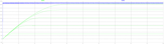
Works perfect while current limit is not reached.
When current is approaching the limit, the output voltage decreases. Good.
But, if the limit is clearly surpassed, the cirtcuit's output goes to a high negative voltage.
Did I miss something??
Elvee, I'll look into your circuit. I still don't fully understand how the depletion mosfet section works.
Attachments
But, if the limit is clearly surpassed, the cirtcuit's output goes to a high negative voltage.
Did I miss something??
Hehe. That elusive constant current source provided for free by LTSpice! Remove the current source and replace by resistor, or build up a CCS with discretes, and woila!
It is a variable CCS feeding the 600K resistor with a current comprised between 50 and 500µA, thus providing a reference voltage for the MOS follower.Elvee, I'll look into your circuit. I still don't fully understand how the depletion mosfet section works.
If you look for (relatively) more elaborate circuits, I have published a number of (tried and tested) designs of series regulators.
SemperFi, yes, that was it. Thanks 🙂
Elvee, how is that 50 - 500 uA range set? The 3.3k resistor?
I understand that the 600k is developing the voltage, proportional to the current.
I'm playing with the simulation, and I see it working perfectly. But I still don't get the bias, and how to set the limits of the current (max and min).
Elvee, how is that 50 - 500 uA range set? The 3.3k resistor?
I understand that the 600k is developing the voltage, proportional to the current.
I'm playing with the simulation, and I see it working perfectly. But I still don't get the bias, and how to set the limits of the current (max and min).
Yes, the 3.3K resistor contributes to setting the current, mostly the upper limit of 500µA (which could be modified according to your tastes, but 500µA seems reasonable enough and problem-free)
The threshold voltage of the MOS will also play a role: think of a simple jFET CCS, it is exactly the same configuration when the wiper of the pot is set to the maximum: only the FET or MOS and the 3.3K play a role in defining the current, the LED being just in series and dropping a volt or two but having no real effect whatsoever.
When the wiper is in the opposite position, the LED voltage becomes preponderant and brings the MOS to near cut-off.
Of course, as with jFETs (also depletion devices), there is some dispersion on the Idss and pinch-off voltage, which is why you will probably need to adjust the LED voltage (using color and die area) to meet the current limits, but fortunately, as parameters are correlated, if you adjust the LED for the right min. current, it will also be OK for the max; current (don't expect an exact 1:10 ratio though).
Another option is to simply solder in place whatever LED you have available, and adjust the 600K resistor for the max. voltage you require: the resulting min. voltage might come as 1/6th or 1/12th, but if it does not bother you too much, it is even simpler.
If you want to be more deterministic, you can use a blue LED and add a trimmer in series with the bottom side of the pot: that way, you will be able to define whatever min. voltage you wish
Good points. Thank you.
Why?
Honestly, I chose 10R for the limiting resistor just because I've seen other similar circuits using that value (for similar current demands). The zener is to avoid the gate to be too high with respect to source.
I'll add a gate-ground capacitor. I just didn't consider stability, as I thought that it was of main concern with LDO topologies, not this classic regulator.
I thought, because I only had the schematics to conclude from, that you had put R1 in series with M1 such that when the current increases and the voltage drop across R1 increases, D1 will start pulling the gate voltage down and thereby reduce current. Without R1, I would have guessed D1 to be a mere voltage clamp.
If your idea had been as I assumed, the 10 Ohm is little impedance for D1 to work with if it has to pinch-off M1. This was why I proposed an increase.
Now the interest in your design is getting massive. I'm sure they will give you good advice.
Yes, the 3.3K resistor contributes to setting the current, mostly the upper limit of 500µA
Is this how you work the source resistor?
idss = 150 mA
vgsoff = 1.5 .. 3.5
If choosing -2.5, I get, for 0.5mA of drain current:
R = Vgs/Id * (sqrt(Id/Idss) - 1)
R = -2.5/500e-6*(sqrt(500e-6/150e-3)-1) = 4.7k
When the wiper is in the opposite position, the LED voltage becomes preponderant and brings the MOS to near cut-off.
I think this is where I'm having trouble. Why is it preponderant?
With such a low current (~50 uA), the LED will be droping so little voltage. I didn't even think that a LED could be used in these situations.
I see that current limit on the lower end is not just a matter of increasing the source resistance. Once you place the wiper in the middle, not only source resistance is higher (3.3k + 50k) but there's also R3 (the other half of the potentiometer's resistance) to the diode cathode. If I remove R3 from the schematic, it doesn't work.
So I'm having trouble to understand this point of the circuit.
YesIs this how you work the source resistor?
.../...
It is preponderant, because its voltage must be close to the cut-off voltage, leaving just a little residue to allow for the 3.3K.I think this is where I'm having trouble. Why is it preponderant?
With such a low current (~50 uA), the LED will be droping so little voltage. I didn't even think that a LED could be used in these situations.
Note that LEDs obey the laws of semiconductors, in particular the I-V exponential relationship: for a 10:1 current ratio, the voltage will vary by 26*ln(10)=60mV: not very much compared to the 1.7V forward drop.
You could use other devices, like a string of diodes, but this would compromise the thermal stability
A better way to see how this work is to consider that the source resistance remains unchanged at 3.3K, but a variable, negative voltage is added in series with the gate, shifting its apparent threshold voltage.I see that current limit on the lower end is not just a matter of increasing the source resistance. Once you place the wiper in the middle, not only source resistance is higher (3.3k + 50k) but there's also R3 (the other half of the potentiometer's resistance) to the diode cathode. If I remove R3 from the schematic, it doesn't work.
So I'm having trouble to understand this point of the circuit.
You could do without the diode, just using a variable resistance in the source, but the variation would need to be large, and you would need a logarithmic potentiometer to make it usable, but it is an option
With a log pot, yes. With a linear pot, turning the knob halfways would make the current to drop to 20%, which is not very comfortable. But log pots are easy to get, that's ok.
Which do you think are the advantages of this circuit over the one I attached in post #6 ? Both use a pot (which is at high potential) to generate a reference voltage, but this one required a depletion mosfet, so I'm sure there's a good reason to use it.
Anyway, you've piqued my curiosity with the LED approach, so I'll look further into understaning it.
I suppose I could use bipolar current mirrors instead of mosfet, right?
Which do you think are the advantages of this circuit over the one I attached in post #6 ? Both use a pot (which is at high potential) to generate a reference voltage, but this one required a depletion mosfet, so I'm sure there's a good reason to use it.
Anyway, you've piqued my curiosity with the LED approach, so I'll look further into understaning it.
The currentmirror MOSFETs used in the sim are not the ones of choice, but the ones I easy find in the sim lib. Do not use those at these voltages.
I suppose I could use bipolar current mirrors instead of mosfet, right?
Depending on the way it is connected, the pot in #6 will see most or the totality of the input voltage across its terminals, which is too much for the majority of regular pots.Which do you think are the advantages of this circuit over the one I attached in post #6 ? Both use a pot (which is at high potential) to generate a reference voltage, but this one required a depletion mosfet, so I'm sure there's a good reason to use it.
With the CCS, the pot only sees a few volts.
The circuit in #6 has zero line regulation, and both circuit should have a similar load regulation (comparable output resistance), except that when you draw current, the input voltage will drop, because the transformer+bridge+cap is not an infinitely stiff voltage source.
Since the reference voltage is simply a fraction of the input, this means that the load regulation will also be affected.
With the CCS, you get a stabilization; I wouldn't call it actual regulation, because there is no explicit FB loop, but it is better than nothing, on a par with a zener-based regulator.
The ripple rejection will also be be better for an identical capacitor, because the CCS has a large dynamic resistance, much larger than the resistive divider.
Yes, Elvee, I agree. Thanks for all this information. It's been very helpful.
I'll try this one on my tester. But for an amplifier, I'd like to keep the potentiometer at low potential.
Do you think it is possible to "merge" your approach with SemperFi's, using a potentiometer which is not at high potential?
I'll try this one on my tester. But for an amplifier, I'd like to keep the potentiometer at low potential.
Do you think it is possible to "merge" your approach with SemperFi's, using a potentiometer which is not at high potential?
Then, your simplest option is a true regulator: one with only two transistors, and an explicit FB loop.
You could try to mess up with a zener-multiplier, but it's not going to be simple or pretty.
Here is an example of such a regulator: the reference voltage is implicit, it is the small MOS threshold voltage, but it works nevertheless rather well, and the tempco is perfectly acceptable.
You could try to mess up with a zener-multiplier, but it's not going to be simple or pretty.
Here is an example of such a regulator: the reference voltage is implicit, it is the small MOS threshold voltage, but it works nevertheless rather well, and the tempco is perfectly acceptable.
Attachments
I suppose I could use bipolar current mirrors instead of mosfet, right?
BJTs or MOSFETs, I just meant do not use 200V rated devices, use 400V or higher rated transistors.
BTW I think I complexed things in the first suggestion. Heres a slightly simpler approach:
Attachments
Here is an example of such a regulator
Elvee, I like that circuit. It is not much more complex, and I suppose it outperforms the previous one. Any drawback compared to the depletion mosfet+diode circuit?
Why C2 between R8/R9, and not a single 66kohm and C2 across input (as I've seen in many other schematics)?
SemperFi, much better 🙂
Except for the pass transistor, I preffer to use bipolars, just because they are not as fragile (ESD). I have MJE5852G and ZTX758 PNP bipolars. Both are 400V collector-emitter, 8 A and 500 mA. But the smaller one is only a 1W device. Do you think it'll be OK for transistor M5? I'd go for a bigger one.
I will try both circuits. They both meet my requirements. Thank you.
- Status
- Not open for further replies.
- Home
- Amplifiers
- Power Supplies
- Simple regulator for high voltage low current