Hi,
I am new to the PCB design so I decided to start from what I thought is a simple task: dual polarity power supply PCB for a chipamp. But now I have a question. Is it OK to place the ground and power traces/planes on top of each other on two different PCB layers. For example V+ trace is parallel to V- trace on same layer but GND is on the other layer below both power traces. Or I should route all three in parallel on the same layer with GND being between V+ and V- ? Could someone suggest which way is better and why?
Thanks,
OlegSh
The Zero Volt trace above/below the +ve trace achieves low loop area.
Similarly for -ve trace.
If the PCB is very thin then you get even lower loop area.
This is where multi-layer PCBs win. The layer can be <10thou/mil apart for lowest loop area and lowest impedance AND they gain a little bit of capacitance due to trace area and small gap.
All three side by side is not as good. Better would be a twisted triplet of +ve -ve zero volts, for good Flow and Return loop area AND cancellation of (more distant) fields due to the twisting.
Worst of all are the +ve trace separated from the zero volts trace and then both separated from the -ve trace.
This is the way you see most PSU and amplifier PCBs laid out. A disaster !
Yes multi-layer boards do this.
6 or 8 layers (and many more) and approximately half of them are non signal planes.
6 or 8 layers (and many more) and approximately half of them are non signal planes.
My point was more to the OP's situation. Rather than running 0 volt traces does it not make sense to run a ground plane on top and bottom of the board?
A wide trace under the +ve trace is effectively a plane.
It allows the Return current route to exactly mimic the Flow route.
You can do this manually by overlaying the traces, or you can adopt a local plane, or you can adopt a global plane.
BUT in all three cases, the RETURN ROUTE must exactly mimic the FLOW ROUTE.
This minimises impedance of the whole Flow AND Return route.
One of the biggest errors in laying out a ground plane made by anyone that does not understand ground planes, is forcing the Return Route to NOT follow the Flow Route.
Even though I am responding to questions on using or abusing ground planes, I know that I do NOT have sufficient knowledge to design a multi-layer planed PCB.
I know my limitations.
I am proud that I know NOT to hide MY LIMITATIONS.
I had work colleagues that were the opposite. I would not stake my safety, nor my life, on professionals that tried to operate outside their area of expertise. In my work related experience, Chartered Architects are among the worst for this alleged failing.
Now I must have offended many hundreds of Members.
You can do this manually by overlaying the traces, or you can adopt a local plane, or you can adopt a global plane.
BUT in all three cases, the RETURN ROUTE must exactly mimic the FLOW ROUTE.
This minimises impedance of the whole Flow AND Return route.
.
I guess I am struggling to understand how the critical condition you specify is met when the 0 volt is a copper fill 'ground plane' i.e. the entire board layer area (let's consider just 2 layers for ease) unused by the +ve (or -ve) "flow route" on both the top and bottom layer.
(To aid conveying what I mean by copper pour ground plane see here from the 5 minute mark.)
Andrew, when I have gone to the university to study "Information Theory" 40 years ago and have been taught, how to layout PCBs (using wire-wrap technology): one of the major rules has been to avoid "stray capacities".
I am currently using a PSU-layout, shown in the picture below.
And I think: it is not bad at all.
Best regards - Rudi
I am currently using a PSU-layout, shown in the picture below.
And I think: it is not bad at all.
Best regards - Rudi
Attachments
Last edited:
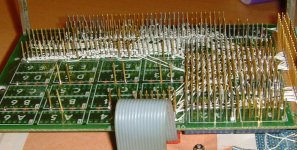
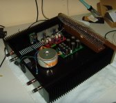
Find attached a picture of this PSU in a beautiful wooden case, featuring a TO3-SYMASYM (what else?!).
Best regards - Rudi
P.S.: The PSU shown above serves as a "Backend-PSU" only.
I have derived a "CAP-Multiplier Frontend-PSU" from the backend on this PCB..
Best regards - Rudi
P.S.: The PSU shown above serves as a "Backend-PSU" only.
I have derived a "CAP-Multiplier Frontend-PSU" from the backend on this PCB..
Attachments
Last edited:
... one of the major rules has been to avoid "stray capacities".
...
IMHO power supply filter banks do not need that rule.
Quite the opposite.
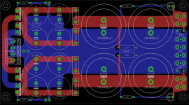
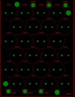
Green, bottom, common or GND
Blue is top + and -
🙂
Attachments
Well Dug, the question is: do our different opinions concerning the layout of the PSU - voltage layers really matter in real life?
Maybe: they do not! 😀
Best regards - Rudi
Maybe: they do not! 😀
Best regards - Rudi
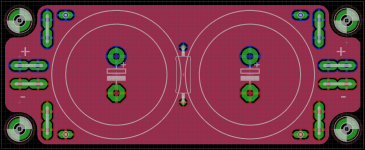
Attached is the two layer filter caps PCB that I just sketched. Layers are identical, one for V+ another for V-. One board is for two 35mm snap-in caps (one rail). The bridge rectifier will go off board. Two boards can be connected to form star ground between them while small size (100x40 mm) allows to put them flexibly withing the chassis.
Attachments
Well Dug, the question is: do our different opinions concerning the layout of the PSU - voltage layers really matter in real life?
Maybe: they do not! 😀
Best regards - Rudi
LOL as they say...I can't argue with that.
There are many ways to ...
🙂
Even though I am responding to questions on using or abusing ground planes, I know that I do NOT have sufficient knowledge to design
a multi-layer planed PCB. I know my limitations. I am proud that I know NOT to hide MY LIMITATIONS.
I've done a few 4 layer boards for clients. They're actually easier to do than 2 layer boards. All the +/- connections just drop right to their own planes
instead of having to be routed, so there are many fewer traces. Either through-hole pads connect directly to the +/- planes, or if smt a short trace goes to a
via doing the same. At 4pcb, you can get a 4 layer pcb (up to 30 sq. in.) for $66. Osh Park is good for smaller pcbs.
Nice to see a separate power supply pcb.
This keeps ground loop problems to a minimum.
I once designed a USB mixer with power supply on the same pcb as the audio.
With shorted inputs I got 1 volt of hum on the output !
I had mixed the power supply and audio grounds randomly.
On the next pcb revision I separated the power supply and audio completely.
The power in and out went through the power supply only.
This time there was almost zero hum on the output.
The smoothing capacitor charging pulses modulate the ground line and can cause havoc.
...
At 4pcb, you can get a 4 layer pcb (up to 30 sq. in.) for $66.
...
You have to buy 4 minimum...$66 each, $10 handling plus shipping.
🙂
Last edited:
You have to buy 4 minimum...$66 each, $10 handling plus shipping.
🙂
If you're a student, only one pcb is ok.
If you're a student, only one pcb is ok.
There are numerous Chinese companies who will supply small quantity pcb's at very good prices.
The one I use does have a min order of 5 but the price is about £80 including shipping to the UK. The turn around from order to getting the pcb's is about 2 weeks.
- Status
- Not open for further replies.
- Home
- Amplifiers
- Power Supplies
- Simple power supply PCB layout question