I quite like a slightly overcompensated Vbe for the output stage............In my latest Mosfet amp the output bias starts at ~250mA per device and at the hottest temperature measures ~150mA. A little trial and error might be in store to dial it in to stable operation. Others might dissagree with this but it works for me.🙂
It helps keep the output stage from overheating in hot weather and if I ever drive the amplifier to excessively high heatsink temperatures.
Since your have a lot of over comp in a VFET output stage, I think you have nothing to lose and the gains are in your favour.
Quick warm up.
Sounds good at first start up.
Self protects when it is very hot.
Still trying
That VBE circuit with my original circuit (original circuit picture attached) did not worked so fine. So I have tried the VBE circuit Andrew posted. It worked much better. Before taking any further action I would like to simulate the circuit. I have tried the LTSpice IV, but found it very difficult to work with. I don´t know if there is a demo of Electronics workbench that I can use to simulate the original circuit with the VBE circuit Andrew has sent.
Andrew,
It would be nice if you could send me the files from your circuit in LTSpice format, so I could simulate the circuit with the power supply of +60v and -60V. My e-mail is eltongp@gmail.com.
Regards,
Elton.
Attachments
Hi,
which Andrew? Which post?
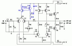
The blue highlight is a CCS.
There is no Vbe multiplier for the output stage.
The output bias is set by the voltage across the variable resistor.
This output stage can only operate reliably with Lateral mosFETs.
which Andrew? Which post?
The blue highlight is a CCS.
There is no Vbe multiplier for the output stage.
The output bias is set by the voltage across the variable resistor.
This output stage can only operate reliably with Lateral mosFETs.
@ Eltongp, I try to suggest you to improve current source for the input differential amplifier ... there was no word about VBE multiplier. 😕
Tekko VBE
Sorry Andrew,
It was acctualy Tekko who posted the VBE circuit that I have inserted on the original circuit. Post #5. I got myself confused with so much help from you all (which is a nice thing).
I will create the file for the circuit with the modifications in LTSpice. My doubts will be about simulating the circuit and measuring the needed voltages.
Tekko could you send over your files in LTSpice format?
Regards,
if you want to send private attachments then you must use the Email, not the PM.I will replace the P2 of my original circuit by the VBE circuit (Q8, R2, R13 and C8) Tekko has sent.
It worked !!!!!!!
It looks like I am getting somewhere....
After a few changes here and there and some more burned components , the circuit is working with only 2 mosfets (1 IRFP240 and 1 IRFP9240) on +60v and -60v😀.
I couldn´t test it properly, because it is late at night. No loud sounds allowed at that time😡. Tomorrow I will test it with a speaker (I was just using a punch of resistors on the output).
If the quality of the sound is ok, I will redraw the circuit with the modifications and post it.
I might also change the PCB and post it as well, so everybody who wants to assembly this kind of amplifier can give it a try.
Regards,
Elton.
It looks like I am getting somewhere....
After a few changes here and there and some more burned components
, the circuit is working with only 2 mosfets (1 IRFP240 and 1 IRFP9240) on +60v and -60v😀. I couldn´t test it properly, because it is late at night. No loud sounds allowed at that time😡. Tomorrow I will test it with a speaker (I was just using a punch of resistors on the output).
If the quality of the sound is ok, I will redraw the circuit with the modifications and post it.
I might also change the PCB and post it as well, so everybody who wants to assembly this kind of amplifier can give it a try.
Regards,
Elton.
It worked !!!!!!!
Thats good to hear. Before you crank it out, I think you should work on making the bias stable. Measure the initial bias setting, should be ~200mA or so, and measure it with no load and no signal for a while and see where it tracks. If it begins to increase, you will need to adjust the Vbe multiplier. If it begins to decrease, then first place full swing signal with NO load and verify that there is no change in it, AC or DC. If that is OK, then push the signal into clipping with no load and verify there is no or very little change in bias. If this test is successful, then place a resistor load on it and crank it out in order to heat the outputs up. Remove the signal and load and imediatly measure the bias and compare it to the initial.....
So far so good
After a few tests it seems it is all working fine. I will have an osciloscope today and will perform some stress tests. With the osciloscope I will be capable of measuring the real wave form, so I will set bias and offset to the best waveform results. I will post the results in terms of adjustments and output power.
I am posting the final circuit, so you all can have a look at it.
Regards,
Elton.
Attachments
Two suggestions:
- there are certainly missing two 100 uF/100V parallel to 100 nF caps from chatode D1 and anode D2 to ground, no explanation needed
- maybe you should left VT5 from post #15 in the circuit?
Nice amp though. 😉
- there are certainly missing two 100 uF/100V parallel to 100 nF caps from chatode D1 and anode D2 to ground, no explanation needed
- maybe you should left VT5 from post #15 in the circuit?
Nice amp though. 😉
Change R1 to 27K, the same as the feedback resistor and R2 to 1K. The of-sett will be better and the currents shared by the LTP will be more balanced. This amp can compete with the Goldmund any time.😀
Nico
EDIT: P1 could be much smaller, maybe 100 - 200 Ohms as P1 also functions as degeneration resistors.
Nico
EDIT: P1 could be much smaller, maybe 100 - 200 Ohms as P1 also functions as degeneration resistors.
Last edited:
good suggestion from Nico.
But first check by adding a 100k pot wired as a variable resistor across the 47k.
adjust the 100k down while monitoring the output offset. You will probably find that 47k//VR will not be near 27k. This is because there is an adjustment pot in the tail of the LTP. That creates another output offset.
The Tail pot must be set to exactly midway, leaving emitter degeneration resistor values of 500r each. No wonder it manages with 18pF of compensation, it has very little gain to feedback.
Then readjust that 100k pot to reset output offset. You can replace the pot with a fixed resistor of the same value as the pot, or you can replace the 47k//VR with a fixed resistor that equals the // combination.
I would leave the 47k in place and tack on a // resistor underneath the PCB. Easy to undo later and saves the risk of damaging the PCB now.
The other advantage of Nico's suggestion is that a lower Rin drops the High Pass filter RC down to a more compatible value to match the NFB RC value.
After changes
After doing some of the suggested changes (P1 to 100R, R1 to 27K, R2 to 1K, 100uF and 100nF capacitors added), the stress test was nice. I mean nice for me and very bad for the neighbors. At 1KHZ and 1Vp input signal the amplifier was capable of producing 175W at 8 ohms with the perfect sine wave measured on the oscilloscope.
In 4 ohms the output power was 330W. For each test (8 and 4 ohms) the system was on for 30 minutes.
As you may imagine, a good heat sink is required under this stressful situation. In 8 ohms the heat was not so bad. Just one regular size fan was capable of properly refrigerating the heat sink.
In 4 ohms, 2 fans were needed. One sucking up the air and another one pushing the hot air out. Even so the heat sink was a little bit hot at the end of the tests. In that sense I strongly recommend the usage of 4 output transistors and a big enough heat sink for usage in 4 ohms.
I will post some pictures of the final circuit (without the case because I haven´t make it yet). I have changed the PCB in order to reflect the changes of the circuit and make possible to use 4 transistors. The only problem was with the zener diodes. Unfortunately they will have to be soldered either on the output transistor leads or underneath the PCB.
I will produce the new PCB and will post the pictures.
I would like to thank you all for the helpful advices. I could not have it working without your help.
Regards,
Elton.
Hi
With ~9.5mA of current in each leg of the VAS differential, 100R degeneration may be a bit large. Perhaps 10R to 20R would be better for R8 and R9. Also with 10K, 9.5mA would be 95V. This means there is not the same Vce across the VAS differential transistors, assuming the differential is balanced, and it should be.
I added some small changes to your circuit you might consider, those suggested by others here are good as well. The purpose of the extra MJE340 cascode with base tied to GND is so that there will be the same voltage across the differential VAS transistors. This means Pd will be the same so that DC bias will not drift. If one device is hotter than the other, Vbe will be affected and it will conduct more current with the same bias settings. Another improvement would be to use a Wilson mirror.😉 Then you can use small signal devices for Q3 and Q4, and the third transistor could be the MJE350. If you could obtain a matched array for Q3 and Q4, it would be best, but you could always hand match. The idea of degeneration is to make the % difference in the two transistors less. The drawback is that degeneration is a form of negative feedback and reduces the gain of the devices. Trade-offs is the norm in electronic design. Pick the best trade-off for the application. In the case of a mirror you would seek matched characteristics.
Next steps for improvement might be to be able to get full voltage swing from the outputs. Notice the output stage can only swing the rail voltage minus a few volts lost in the differential, minus voltage across R22/R23 and D1/D2, minus Vgs Th of the output devices, minus the extra Vgs required for conduction of the output devices. Datasheet will help to determain this. Notice it will not be the same for N-ch and P-ch of the devices your using because they are not complementary and have different transconductances.
One step at a time though, eh?
Attachments
![schematics2[1].jpg](/community/data/attachments/184/184273-335ffec0fb3bd5ee8c67ee1bbd3cbf62.jpg?hash=M1_-wPs71e)
Last edited:


- Status
- Not open for further replies.
- Home
- Amplifiers
- Solid State
- Simple mosfet amplifier