Here are some examples of simple, cheap, medium performance regulators.
Elvee, could your design be modified to output a variable voltage selected by the user? For example if you wanted to make a test bench power supply that would output 0 to 500V from anywhere between 0 and 500 mA?
Unfortunately, no: these regulators are intended as adjustable HV regs, the high voltage equivalent of a 78xx regulator, and making them fully variable would pose serious problems and mostly negate their advantage of simplicity/cost/performance mix.
I have described another fully variable supply combined with an original switching preregulator, make a search on this forum.
I also have in my files a fully fledged lab variable supply, but it is a monster having 0 to 700V and 0 to 1A capability, perhaps a bit much compared to what you have in mind.
Hi. If I take the schematics from your post 14, how are the resistors calculated ? I have an input voltage of 115-0-115V and need an output of 140V.
Thanks and best regards
Christoph
Thanks and best regards
Christoph
An input of 115V is not exactly plentiful for a 140V regulated DC: it yields ~160V raw DC, if the AC value is exact.
It is sufficient though, and here is an example with the component values adapted.
R1 has been altered too, to take into account the relatively small regulation margin.
If you want to make it adjustable, you can insert a trimmer at the junction of R4 and R5, just as in #14
It is sufficient though, and here is an example with the component values adapted.
R1 has been altered too, to take into account the relatively small regulation margin.
If you want to make it adjustable, you can insert a trimmer at the junction of R4 and R5, just as in #14
Attachments
Hi, thanks for your quick answer. Don't know if my brain is too tired, but if i have 115-0-115v on the transformer, doesn't this mean 230v ? If i put the center tap to ground ?
Regards, Chris
Regards, Chris
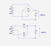
Knowing what this will be used for... you must use the transformer with the CT grounded (bottom illustration), or you won't have enough current. On the other hand, you'll be fine with 130vdc, which gives you a bit more margin.
Elvee,
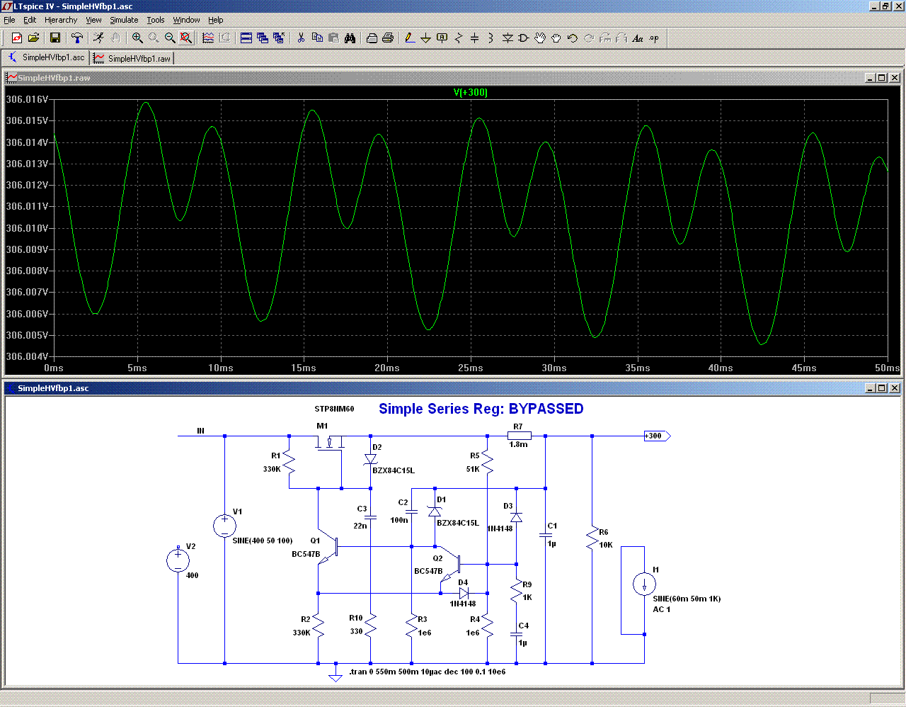
I've been studying your circuits and I believe I understood most of it 🙂 However, one thing that puzzles me still is the compensation parts to the "left". I am talking of this circuit as a reference:
http://www.diyaudio.com/forums/atta...201334-simple-hv-series-regulators-ssrby1.gif
(Bypassed regular version)
I understand that C3 and R10 interact with the mosfet gate charge / capacitance and R1 as well, and I can find empirically values to provide optimum rejection, but I do not really understand how they are supposed to work really and how to calculate them upfront.
Can you, or anyone, shed some light on this?
Otherwise, great circuits, thnx
GR
There is a number of ways to view this network: one is as a shunt compensation in parallel with Q1 which is the VAS, but it can also be seen as a Miller cap viewed from the MOS.
It is connected between ground and gate, but of course the drain and V+ are at the same AC potential as the ground, at least from a loop stability perspective.
For the input ripple, matters are different, which is why it has to be connected to the ground: it not only compensates the regulator but also help rejecting the hf ripple, thus killing two birds with one stone
An interesting attribute of this location for compensation is that there is no additional pole created: the already dominant pole is just reinforced, which means it doesn't have to be as overwhelmingly dominant as if a completely new one had been created
Last edited:
Thanks,
but how do you size the cap & resistor? I found by try & error that apparently the actual values don't matter too much. R1, the mosfet bias resistor plays a much bigger role..
One more question, why do you have to connect the bjts and protection diodes directly to the output node, downstream of R5 (and the "virtual" resistor)? Sorry I am not a psu or HF expert...
greets
GB
You have to estimate the transfer function of the diff amp Q1/Q2 cascaded with M1 in common source (yes, it doesn't look obvious, but that's how it is connected) and make C3 large enough to shift down the curve so that the unity intercept point is in the clean, 6dB/octave section, far from the higher frequency poles; admittedly not an easy task considering that the circuit is somewhat, let's say "involved" and that many secondary effects, including dynamic ones play a role.Thanks,
but how do you size the cap & resistor? I found by try & error that apparently the actual values don't matter too much.
You can get a rough idea of a starting point using back-of the-enveloppe calculations, but then it is necessary to use the sim to optimize the circuit.
It does play an important role: it is directly related to the open-loop gain and the low frequency cornerR1, the mosfet bias resistor plays a much bigger role..
For the protection diode, it doesn't really matter, but for the rest, that is what creates the output impedance compensation: try connecting them the other way round, and you will see a substantial increase of the output impedanceOne more question, why do you have to connect the bjts and protection diodes directly to the output node, downstream of R5 (and the "virtual" resistor)? Sorry I am not a psu or HF expert...
I have described another fully variable supply combined with an original switching preregulator, make a search on this forum.
I had forgotten about this thread!
I didn't end up building your variable supply. I wanted a dead-simple linear supply that was fully adjustable and offered decent regulation. Mine ended up supporting up to 490V and up to 300 mA.
I started with the basic Maida approach using the LM317, but instead of using power transistors as the predrop devices, I used 6550 power tubes. This works well. It has rudimentary current limiting provided by the pentode screens. And because the LM317 is used, it offers pretty good voltage regulation. It does not offer user adjustable current limiting, but will handle a short circuit with no problems.
- Status
- Not open for further replies.
- Home
- Amplifiers
- Power Supplies
- Simple HV series regulators