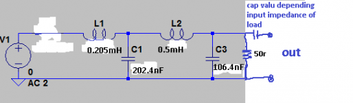
Attached the LPF I use first pic left.
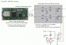
I expected minimum the same output 0.56Vrms at 0dBfs as audiodesign web http://www.audiodesignguide.com/PureDSD/ 2nd pic right
I expected minimum the same output 0.56Vrms at 0dBfs as audiodesign web http://www.audiodesignguide.com/PureDSD/ 2nd pic right
Attachments
Is the DAC output level now still the same as it was starting back in 2019? IOW, has anything changed?
I was & still try to implement the just gain to reach the 2Vrms, but it's difficult without knowing the real output....
rfbrw
Yes I this is true. I have been looking at it some time ago. Only supports up to 256 DSD direct and 128 DoP. That could be a problem. But otherwise you are right and I should probably try it.
Thanks.
Yes I this is true. I have been looking at it some time ago. Only supports up to 256 DSD direct and 128 DoP. That could be a problem. But otherwise you are right and I should probably try it.
Thanks.
koldby
Member
Apparently there could be a problem with this board and the DSC2, as the MiniDSP board cannot accept external clock in DSD mode, and the DSC2 has onboard clock generation and therefore needs an USB interface that can work in slave mode. Any suggestions to how this can be fixed, so one can use this multi channel USB to DSD interface with the DSC2?That board, as it is being sold, outs I2S. If you want to out DSD in multichannel you need a "special" firmware and flash it to the Xmos. I have tried and works well, but I believe that minidsp offers a ready DSD multichannel : check it out here MCHStreamer - USB Audio Swiss-Army knife - Multichannel PCM/DSD/PDM/ADAT/TDM/SPDIF interface
Haven't tried the mchstreamer though, so cannot comment more on that.
cheers
Quote
Report
[IMG alt="koldby"]https://www.diyaudio.com/community/data/avatars/s/5/5177.jpg?1638973604[/IMG]
koldby
Member
Another problem could be that the board does not support DSD256 in DoP mode but only in DSD direct. Can J-river convert PCM and send it as DSD direct in DSD256? It does not work with the Amanero , only in DoP mode.Quote
Report
[IMG alt="lindamar"]https://www.diyaudio.com/community/data/avatars/s/76/76938.jpg?1638973622[/IMG]
lindamar
Member
And you are right there, I have tried the diyinhk board with a different dac that can work in slave mode. The DSC2, as you mentioned, works in masted mode and that means the USB interface needs to work in slave mode. I have not modded the Xmos firmware to accept an external master clock, but could be done though. Amanero has a firmware that does precisely that. The previous version of the DSC (the one that has no reclocking and oscillators on board) I believe would work.Apparently there could be a problem with this board and the DSC2, as the MiniDSP board cannot accept external clock in DSD mode, and the DSC2 has onboard clock generation and therefore needs an USB interface that can work in slave mode. Any suggestions to how this can be fixed, so one can use this multi channel USB to DSD interface with the DSC2?
LikeQuote
Report
As can be seen there is also a problem when using the DCS2 as the MiniDSP apparently cannot work in slave mode?
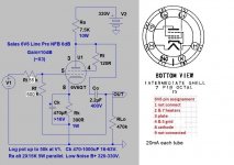
Used severals in my journey:
1- 600-15K OPT
2- 300-15K OPT
3- 5687 SE triode
4- 12B4 SE triode
5- Salas 6V6 SE triode https://www.diyaudio.com/community/threads/6v6-line-preamp.102352/page-230#post-7250754
1- 600-15K OPT
2- 300-15K OPT
3- 5687 SE triode
4- 12B4 SE triode
5- Salas 6V6 SE triode https://www.diyaudio.com/community/threads/6v6-line-preamp.102352/page-230#post-7250754
Attachments
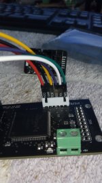
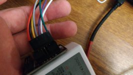
It's well connected?
Where is the Xilinxd license file & Lm license file?
I guess don't need to power the pcm2dsd because is powered by the USB port right?
TIA
Where is the Xilinxd license file & Lm license file?
I guess don't need to power the pcm2dsd because is powered by the USB port right?
TIA
Attachments

Last edited:
Simple DSD Converter needs +5v from somewhere into its power connector. If the LED is not on then it is not powered.
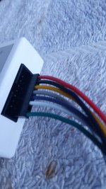
Also, that is not a proper I2S cable. It should have one ground wire for each signal wire. The ground and signal pairs can be loosely twisted together, or ribbon cable can be used with every other wire a ground. What you have there in the pic would be inappropriate even if it were only 1" long. Maybe helpful to remember this is RF, not 20Hz - 20kHz audio going through those wires. They wiring needs to be designed for RF use up to above 100MHz (if we allow for clock edge harmonics, which we should).
Also, that is not a proper I2S cable. It should have one ground wire for each signal wire. The ground and signal pairs can be loosely twisted together, or ribbon cable can be used with every other wire a ground. What you have there in the pic would be inappropriate even if it were only 1" long. Maybe helpful to remember this is RF, not 20Hz - 20kHz audio going through those wires. They wiring needs to be designed for RF use up to above 100MHz (if we allow for clock edge harmonics, which we should).
Last edited:
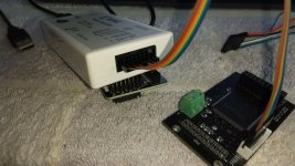
The Xilinx programmer uses a single row of wires, if that's what we were looking at in your pic. When you are programming the FPGA, you still need to supply +5v to the DSD Converter board so that the LED comes on. When the JTAG programmer is connected and talking to the FPGA and also connected to the PC, then its LED light should turn green, at least mine does.
Also IIRC if using the latest version of ISE, you don't need a license to run the Impact program. Are you trying to make it work in Windows or in Linux?
Also IIRC if using the latest version of ISE, you don't need a license to run the Impact program. Are you trying to make it work in Windows or in Linux?
Windows, I'm really lost, I'm a newbie to flash devices except Amanero, also I can't know how Xilinx software works, TIA for help.
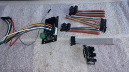
Do you have a pic of cable needed?
Do you have a pic of cable needed?
Looks okay for that use. Just check to make sure the pins have the same names at each end of the wires.
Other things you may need to know about are in a collection of files I saved in my dropbox: https://www.dropbox.com/sh/fht6iktll3wy7nd/AAAM5kERD1Aj4Kz8T_0JAr1Wa?dl=0
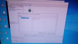
Once you get the right version of Oracle Virtual Box installed, and then install ISE and Impact in Virtual Box, then you will need to have on hand the .bit file you want to use to program the FPGA. First you need to use Impact to make an .mcs file from the .bit file so that the eeprom can be programmed using the .mcs file. The .bit file is used to program the FPGA. To get Impact to create the .mcs file you have to tell it the type of eeprom and its memory size. The eeprom chips specified for this project are I believe all 8MB capacity. In any case the eeprom part number will tell you the size.
Note: the other thing I found was that if I had an external USB hub attached to the PC, it would crash Impact. So I disconnected the hub and plugged the JTAG programmer directly into the PC.
Another thing to know is that Virtual Box will take ownership of some USB devices and probably ownership of any CD drive. There are various ways to transfer data into and out of Virtual Box including by using a CDR. You can also set up file shares between, say, for example, the Linux in Virtual Box, Virtual Box, and the host Windows10 PC. It can take a lot of fiddling around though if you aren't familiar with how to do it.
Last edited:
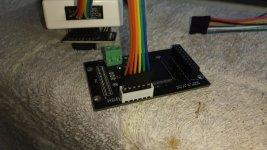
I would recommend you to use the adapter PCB because this is most secure connection, so connect it to Xilinx programmer, there is a single way to fit it there.
You can see on the adapter a single row of 8 pins, and you also have a cable which has 8 female single (monoblock) connector at one end with 7 wires only - this is for adapter side, take care about its orientation - and 7 individual connectors at the other end everyone having a name printed - these are for modulator side.
You have to power the modulator with 5 VCC and of course you should conect the programmer to PC via provided USB cable.
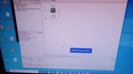
Run Impact software, then "Boundary Scan", then right click and "Initialize chain". You should see your XC6SLX9 chip.
If you are at this point, I can tell you how to write SPI flash chip. (I supose it is still M25P80, if not, tell me).
You can see on the adapter a single row of 8 pins, and you also have a cable which has 8 female single (monoblock) connector at one end with 7 wires only - this is for adapter side, take care about its orientation - and 7 individual connectors at the other end everyone having a name printed - these are for modulator side.
You have to power the modulator with 5 VCC and of course you should conect the programmer to PC via provided USB cable.
Run Impact software, then "Boundary Scan", then right click and "Initialize chain". You should see your XC6SLX9 chip.
If you are at this point, I can tell you how to write SPI flash chip. (I supose it is still M25P80, if not, tell me).
Attachments
Checked, thanks.Looks okay for that use. Just check to make sure the pins have the same names at each end of the wires.
Okay, and you have the .bit file available for Impact to use?
If so, then you need to choose the option to create a PROM file (which it will do from the .bit file).
BTW once you have both files there is a Wizard that will take you though loading both devices, the FPGA, and the eeprom. Although you could probably go ahead and load the .bit file into the FPGA at this point. If you don't have the .bit file maybe you could burn it onto a CD that can be read from within Virtual Box?
If you don't know which devices Virtual Box has taken ownership of, then look at the Virtual Box menu at the top of the overall window. Its a little above the Impact window menu bar.
Last edited:
- Home
- Source & Line
- Digital Line Level
- Simple DSD modulator for DSC2