The hardest thing to do is the tweeter amp.
Hi Telestar
I wouldn't like to spoil Soekris thread but I'm very interested if You could tell more about your solution.
Rosendorfer
Hi Telestar
I wouldn't like to spoil Soekris thread but I'm very interested if You could tell more about your solution.
Rosendorfer
Hi Telestar
I wouldn't like to spoil Soekris thread but I'm very interested if You could tell more about your solution.
Rosendorfer
Send me a PM.
Sumaudioguy,
Tell me how and I'll test it and fix it, assuming it's actually something it would meet in the real world...
I have the opposite view, signals coming back and mess with the feedback, don't happen without feedback....
Thanks, I'll update as things progress.
Soren
Beg to differ- I can make that thing oscillate in a heartbeat, no problem at all. Been there done that.
Tell me how and I'll test it and fix it, assuming it's actually something it would meet in the real world...
I like no global feedback for circuits driven by and driving know impedances especially at RF frequencies or for extremely low noise. Speakers are not even loads but in stereo pairs one speaker makes the other speaker produce a signal so a speaker is another source. This means the amp needs to be a little more robust than the one shown.
I have the opposite view, signals coming back and mess with the feedback, don't happen without feedback....
Lots of luck with it though. Will be curious to see the finals. Congratulations on the efforts!
Thanks, I'll update as things progress.
Soren
Hi , how the overal gain of this amplifier is calculated (open loop)?
Thnks
The gain of the Voltage Amplifier is ((R18||R39)/2) / (R37+2(1/Yfs(fet))). It then have to be multiplied by Output Current Buffer Gain, typically *0.95.
Simplified to Gain= (R18/(R37+100))*0.95.
Soren
Here are some suggestions then:
1. The current limit circuit is not quite right. Look of the original Leech amp and see how it was done there. It is only slightly different though. I could have a miss on this but believe it takes two more diodes and two more caps.
2. See the watt burner fireball series for details on this. Loads are reflected upstream through emitter followers real well. This means Q11 see the beta reduced version of the load. That stage needs to have as much current flowing through it as is practical to drive the bad load. Use as much current there as the transistors will handle. As it appears to be common base the bandwidth is going to be very wide. You may wish to use slower transistors. Wideband parts means driving the wideband load. Not so much bandwidth means not so much load at high frequencies. Just consider this,
3. C22 needs to be more like 68 microFarads to stabilize the voltage there.
4. C24 needs to be like 1000µF to handle the audio frequency range and current variations there. Have used 100µF in that position and blown them out so now using 1200µF in similar circuit
5. Use a diode and resistor in series for instead of R27.
These are things to think about. Using a lot of common base and common gate stages is great for bandwidth and linearity but that bandwidth can bite you badly because bandwidth also means way more signals to process. With open loop power my results were better with slower parts. Maybe you could also consider adding another low pass filter inside the circuit somewhere to slow things down.
Any of this might not be exactly right for what you are doing but do represent some experience. If it is not slowed down somehow it will be very easy to make oscillate. Probably no more the 20 volts per microsecond slew is needed anyway so whatever you can do to slow it down and still keep gain stable will probably help.
Still good luck.🙂
Probably no more the 20 volts per microsecond slew is needed anyway so whatever you can do to slow it down and still keep gain stable will probably help.
I know that nowhere has been measured more than 40V/uS needed. But I believe that in reality a much higher SR is needed and it also let's not forget that it depends on the total power of the amplifier.
Maybe a compromise can be found for Soren amp? 🙂
Here are some suggestions then:
1. The current limit circuit is not quite right. Look of the original Leech amp and see how it was done there. It is only slightly different though. I could have a miss on this but believe it takes two more diodes and two more caps.
The current limiter is correct, there are different ways of doing things. Take a look at Self's and Slone's books, I have them here....
2. See the watt burner fireball series for details on this. Loads are reflected upstream through emitter followers real well. This means Q11 see the beta reduced version of the load. That stage needs to have as much current flowing through it as is practical to drive the bad load. Use as much current there as the transistors will handle. As it appears to be common base the bandwidth is going to be very wide. You may wish to use slower transistors. Wideband parts means driving the wideband load. Not so much bandwidth means not so much load at high frequencies. Just consider this,
Q11/Q21 has enough current to drive 0.5R loads, and since they're current driven anything "coming back" would just go into their load resistors. Can't see any problem.
There are much discussion about how fast an amplifier need to be. I prefer to make the basic circuit fast and then control bandwidth with capacitors, here C20/C26.
Can you provide a link to "watt burner fireball", a quick search didn't find anything....
3. C22 needs to be more like 68 microFarads to stabilize the voltage there.
No, the current though Q16 is pretty constant and Q16 works as "active zener", C22 is only for speedup and don't need to be bigger.
4. C24 needs to be like 1000µF to handle the audio frequency range and current variations there. Have used 100µF in that position and blown them out so now using 1200µF in similar circuit
Again, C24 is just for speedup, basically to empty the BE capacitance, and my breadboard prototype's 900 Khz power bandwidth (without C20/C26) show I'm on the right track 🙂
5. Use a diode and resistor in series for instead of R27.
Could be done to lower the impedance there, even better would be two diodes + resistor but then the current though the drivers are not that precise. But the single resistor is fine, remember that this amplifier is simple....
These are things to think about. Using a lot of common base and common gate stages is great for bandwidth and linearity but that bandwidth can bite you badly because bandwidth also means way more signals to process. With open loop power my results were better with slower parts. Maybe you could also consider adding another low pass filter inside the circuit somewhere to slow things down.
The design principle is exactly a fast and linear amplifier, with bandwidth controlled by C20/C26.
Any of this might not be exactly right for what you are doing but do represent some experience. If it is not slowed down somehow it will be very easy to make oscillate. Probably no more the 20 volts per microsecond slew is needed anyway so whatever you can do to slow it down and still keep gain stable will probably help.
My only problems so far have been parasitic oscillations, remember that the no global feedback removes the main oscillation problem....
Still good luck.🙂
Thanks, feedback is always welcome, there're always room for improvements and I could have missed something 🙂
Soren
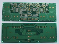
Got the PCB's....
Just received the PCB's, 3 oz copper with immersion gold, looks pretty good 🙂
Have the parts in the mail from US, boards should be mounted in a week or something....
When choosing PCB manufacturer for the prototypes I first looked at local EU manufacturers, seemed pretty expensive once you wanted 3 oz copper and gold....
Then I looked at a couple of US manufacturers I have used before, much better, maybe half price....
But some in here recommended PCBCART, a China based prototype PCB manufacturer, so I checked them out, cost now came at about half the US price so since it wasn't an important computer board I decided to use them for this project.... And I'm very happy with the result.
Soren
Attachments
http://www.diyaudio.com/forums/solid-state/154070-watt-sucking-fireball-series.html is the thread.
It is your design so we can agree to disagree. I still hold with #3 and #4 as currents there are much higher than expected. It should be a small current but reality came up with an over one amp for #4 at capacitor C24 with very similar circuit tested.
Early in my amplifier design thought a lot of trouble was parasitic oscillation but that was incorrect view. Most of the time it was beta reflected load back to the oscillating stage or the output was acting as a single port oscillator. Think this- output is capacitive and input is inductive and power applied to the collector. Adding base resistors makes the problem move to a higher frequency but does not fix it, actually makes it worse as input impedance to the stage is higher so more easy to oscillate. My rule- never use base resistor in emitter follower stage as it makes everything worse.
The main source of oscillation in amplifiers is not due to feedback so I disagree. The main source is inadequate drive to the output stages as described in the previous paragraph and watt sucking fireball thread and that oscillation occurs with or without global feedback. There was a thread on simulation of the Adcom 555- an amp that will break into oscillation and then stop (controlled by feedback) because of these exact problems. The other members of the thread did not care for my comments as they were emotionally invested in that unstable amp so I left the thread. Driving a resistor it was quite stable but any bad load and oscillations comes and goes.
As for #5 come on please- this amp has more parts than you can shake a stick at and one more diode improves thermal response and lowers impedance there. An easy change and it makes no sense then to simply use a resistor where a resistor and a diode will work better and is so easy to install.
As for #2 Q11 has a 75 ohm resistor in the emitter so really doubt the part about driving a 0.5 ohm load to full scale. Did I read your comment wrong? Collector load impedance is always higher (without feedback) than the load at the emitter so believe I can safely say the output impedance of that stage is more than 75 ohms. This is very likely the source of oscillation you are finding and attributing to parasitic conditions. Also this method of load compensation usually works better if the capacitor C20 is returned to the plus supply and C26 returned to the minus supply as ground is distant from the transistor Q11 and V plus is very close to the emitter making a good path for the high frequencies which are being shunted off. Remember "in theory" the V plus, ground, and V minus are all tied together with zero impedance between them so it matters not "in theory" where the capacitor shunt is placed. However, in practice this is quite a different thing so use the plus and minus rails.
As for the current limit circuit around Q14, analyze the voltages when the output is near the minus rail. Even with the divider R15 R20 the voltage at the base may push the Q14 into emitter reverse bias. I did not calculate everything out but off hand it looks like it may go reverse bias. I need to check the links you provided and thanks for that.
Glad you received your PCB and hope the work progresses without to much smoke! Good fortune in this design. 🙂
Complete different design, can't see anything relevant, so far I'm very happy with what I have....
It is your design so we can agree to disagree. I still hold with #3 and #4 as currents there are much higher than expected. It should be a small current but reality came up with an over one amp for #4 at capacitor C24 with very similar circuit tested.
High currents, yes, but for a very short time, that's why I want a NP0 cap there....
My rule- never use base resistor in emitter follower stage as it makes everything worse.
Respectfully disagree.
As for #5 come on please- this amp has more parts than you can shake a stick at and one more diode improves thermal response and lowers impedance there. An easy change and it makes no sense then to simply use a resistor where a resistor and a diode will work better and is so easy to install.
I look at every single part, if not needed it don't go in. I believe that the res/cap combo is good, which by the way 95% of the worlds amps with EF output stages also do. Not that I just follow others....
As for #2 Q11 has a 75 ohm resistor in the emitter so really doubt the part about driving a 0.5 ohm load to full scale. Did I read your comment wrong? Collector load impedance is always higher (without feedback) than the load at the emitter so believe I can safely say the output impedance of that stage is more than 75 ohms. This is very likely the source of oscillation you are finding and attributing to parasitic conditions. Also this method of load compensation usually works better if the capacitor C20 is returned to the plus supply and C26 returned to the minus supply as ground is distant from the transistor Q11 and V plus is very close to the emitter making a good path for the high frequencies which are being shunted off. Remember "in theory" the V plus, ground, and V minus are all tied together with zero impedance between them so it matters not "in theory" where the capacitor shunt is placed. However, in practice this is quite a different thing so use the plus and minus rails.
I'm talking about the whole amplifier, it will of course not drive 0.5 ohm to full scale as that would be close to 100A, but it will drive very low impedances with the current limiter being the limit.
Output impedance of the voltage amplifier section is R18||R39, as I use high beta transistors in the current amplifier section the output impedance ends out very low, I have measured the breadboard prototypes to 0.4 ohm with just a single pair of output device, with 2 sets it will be around 0.25 ohm. I'm happy with that.
The current design have no oscillations, C20/C26 is not to control oscillation but to slow down the amplifier, therefore it's correct to connect them to gnd.
As for the current limit circuit around Q14, analyze the voltages when the output is near the minus rail. Even with the divider R15 R20 the voltage at the base may push the Q14 into emitter reverse bias. I did not calculate everything out but off hand it looks like it may go reverse bias. I need to check the links you provided and thanks for that.
I have, Q14/Q19 will not be reverse biased, D5/D6/D14/D15 controls things....
Glad you received your PCB and hope the work progresses without to much smoke! Good fortune in this design. 🙂
Thanks, hey, smoke is part of the fun, that's why I built things, not just simulate 🙂
Soren
Am excited to see the test results with images of scope traces on bad loads and distortion numbers and so on. Hear is my "cheap amp" results for reference. http://www.diyaudio.com/forums/chip-amps/163385-so-just-how-good-can-chip-amp-9.html
Hi Soren, those PCBs look to be of very high quality. I think i'd be happy to 😀But some in here recommended PCBCART, a China based prototype PCB manufacturer, so I checked them out, cost now came at about half the US price so since it wasn't an important computer board I decided to use them for this project.... And I'm very happy with the result.
Soren
Have fun with all the smt components going on it 🙂
Looking forward to seeing how it all pans out..
Mark.
Am excited to see the test results with images of scope traces on bad loads and distortion numbers and so on.
Like this, in sequence:
20 Khz square, 40V pp into 8 ohm || 1 uF
50 Khz square, 25V pp into 8 ohm || 1 uF
20 Khz square, 40V pp into 1 uF
50 Khz square, 25V pp into 1 uF
50 Khz limited by my lab power supply. And it's just a testbench with flying leads an other bad stuff....
See also my recent post:
http://www.diyaudio.com/forums/soli...er-mosfets-2sk3497-2sj618-little-testing.html
Soren
Attachments
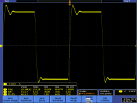
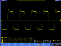

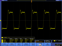
That looks pretty good. With the digitization and pixels size cannot see the detail I would like but will say again that looks pretty good. Have you tried this with loads starting at like 100pF, then 300pF, then 1000pF on up to the 1µF? That is what I do with square, sine, and triangle waves. The worst load is not necessarily the one that will cause oscillation. Will be happy to wait for the finished version and all the measurements for output Z versus frequency, THD, and the annoying load testing with both inductance and capacitance. Fully characterized means fully known, "A filter with gain."
By the way, the watt sucking fireball series discusses a lot of amplifier topologies and methods and is not limited to one design.
By the way, the watt sucking fireball series discusses a lot of amplifier topologies and methods and is not limited to one design.
Analysis of last voltage gain stage and compensation scheme
One of the primary reason for oscillation in power amplifiers is the last voltage gain stage output has increasing impedance with increasing frequency which at some frequency does not provide sufficient drive to control the first driver stage resulting in oscillation. Because the last gain stage usually has lots of gain, the frequency where impedance begins to rise is fairly low. You have used common base last gain stage which is a good idea and have presented a clever way to bias the common bases. Though the bandwidth of this arrangement is clearly much wider than common emitter this design still has rising impedance with frequency. I see two sides, Q11 Q21, each about 3500 ohms output impedance, 1750 ohms Q11 Q21 taken together, with two 33pF, C20 C26, capacitors to ground. Based on those number that puts the corner frequency about 1.3MHz which is likely close to where a normal feedback amplifier would oscillate or, even an amplifier without feedback, due to rising last gain stage impedance. If the last gain stage impedance becomes to high any amplifier will oscillate under some load. But your amp has shunt capacitors to ground, C20 C26, which causes the impedance at that point to decrease from 3500 ohms at 1.3MHz at -6dB per octave instead of increasing as in many other amplifiers. The result is the last gain stage has lower and lower impedance as frequency increases. This will stop oscillation if the corner frequency is low enough. We can clearly see this first order effect in the post of the 10kHz square waves because the period of overshoot and ring become shorter as it becomes smaller. With second order the period remains the same.
In the end you have a compensation scheme and a final gain stage with some pretty nice features. To use such a stage with feedback could be possible if the compensation scheme does not result in to much delay to apply global feedback. I may try this someday if you do not object. There are also a lot more choices for compensation than the one you chose so there may be a topology to benefit from some of the concept and still allow global feedback. In the end....
Very nice.
Wish I could hear it.
You have used common base last gain stage which is a good idea and have presented a clever way to bias the common bases.
I like it, the key is to select LED's with low impedance and NOT paralleling a capacitor as that will create a colpitt oscillator...
I see two sides, Q11 Q21, each about 3500 ohms output impedance, 1750 ohms Q11 Q21 taken together, with two 33pF, C20 C26, capacitors to ground. Based on those number that puts the corner frequency about 1.3MHz
I don't know where you get the 3500 ohms, the output impedance of the voltage amplifier stage is basically R18||R39, with the 10K7 in the 110W version it will give a -3db cutoff of 450 Khz....
In the end you have a compensation scheme and a final gain stage with some pretty nice features.
I still don't consider it compensation, the amplifer is perfectly stable without C20 & C26....
To use such a stage with feedback could be possible if the compensation scheme does not result in to much delay to apply global feedback. I may try this someday if you do not object. There are also a lot more choices for compensation than the one you chose so there may be a topology to benefit from some of the concept and still allow global feedback. In the end....
Plenty of possibilities there, I have actually also been experimenting with the concept of a discrete opamp, see:
http://www.diyaudio.com/forums/solid-state/156674-my-take-buildable-discrete-op-amp.html
Also, I have recently looked at some old HP function generator manuals to see how they did their output amplifier, and what did I find ? The HP 3314A use the same folded cascode voltage amplifier circuit that I use, with a diamond buffer output stage....
Wish I could hear it.
I have a small local assembly house where I live, will probably make a batch of boards when I'm done fine tuning the prototypes....
Soren
You do not include the impedance of the first driver stage in parallel with R18 R39? No matter.
I do not believe the amp can possibly be "perfectly stable" without some way to control the impedance at the first driver. As stated, if impedance is not controlled at the first driver there is a load that will cause oscillation. I have never seen an exception to this so truly believe this is not one but do not wish to argue. I agree to disagree.
Was looking for an HP and TEK manuals myself just this week as I thought this seemed pretty familiar. Actually the drive stage for a CRT in an oscilloscope.
I used a CA3069 transistor array for my "discrete" cough cough, op amp. Worked far better than expected.
I would like to hear it but do not really wish to own one, thank you. Having built several dozens of open loop power amplifiers and to many dozens of various discrete symmetrical gain stages... just do not do either anymore for audio power. Yes for other applications but not audio. Discrete symmetrical gain stages have to long a settling time for my tastes while exhibiting warm up phenomenon and open loop was always very good in the highs but was not so good down low or lower midrange sounding thin and lacking bass control. Yours may be different though. This is why I wish to try something like this common base gain stage in a single ended high gain high feedback form. Do use a common base stage in the level translator in a power amplifier last built in 2001. Now use that IC thing for almost everything except high end audio and then even for bass, so much gain at 50Hz like 200dB.
Anyway- still the best on this effort. It is very good to see such a design show up on DIY, or anywhere for that matter.
Congratulations again.
-SUM
Hi Soren,
Would you please let me know the types of Q17/Q18 80V Mosfets driven by the APV1121S? I am designing an AC/DC opto-isolated switch (non-audio application), but there is no application note on these photovoltaic drivers available.
Thanks,
Attila.
Would you please let me know the types of Q17/Q18 80V Mosfets driven by the APV1121S? I am designing an AC/DC opto-isolated switch (non-audio application), but there is no application note on these photovoltaic drivers available.
Thanks,
Attila.
Member
Joined 2009
Paid Member
are you sure about the led current 4 ma and 28 ma ? 60V and 1k5 or 215ohms makes 40 ma and 280 ma or do I miss something .Precise link here to the Panasonic APV1121:
Download | Automation Controls | Industrial Devices | Panasonic
It can only deliver few uA's, so to ensure quick turn-on (mosfets have significant gate capacitance) I drive it with a short peak of 28 mA during turn-on, and then steady 4 mA constant current. And as Eva says, it have built-in circuit for quick turn-off so nothing special need to be done there.
Soren
- Status
- Not open for further replies.
- Home
- Amplifiers
- Solid State
- Simple Bipolar Power Amplifier - Non Feedback and Production Ready....