Greetings to the forum.
This idea may be of interest to some of the membership.
simple adaptive bias amplifier, finalized! - audio-talk
Regards,
Norman.
This idea may be of interest to some of the membership.
simple adaptive bias amplifier, finalized! - audio-talk
Regards,
Norman.
I think those TO18/TO92 devices are specific application, TRF type AM tuner chips. Many folk experimented with making simple AM radios based on them, back in the 1970s -80s. Are we all talking about the same topic?...The Ferranti device is ZN414 and/or copies like MK484.....
Did I miss a specification or suggestion for the load inductor in your final design?
Greetings.
I helped the young student with certain aspects of the audio stage of her project including the inductor, the radio receiver section is a simple but effective one transistor reflex design that she had completed before I was involved. It was her development of the amplifier, successfully combining several design ideas that I found remarkable. She is just thirteen years old.
The construction of the load inductor for the amplifier was as follows:- "transteel" silicon steel E.I. lams, 40 × 30mm oa size. 7mm leg section. Gapped with 8 thou" transformer paper
Bobbin wound with 30 swg ECW, eleven layers of 55 turns, with transformer tape every second layer. DC winding resistance @ 3 ohms.
With a suitable op transistor and supply of 6 volts, the amplifier managed an RMS P ave of just over a Watt into 3 ohms before clipping, using the same inductor design.
Norman.
Last edited:
Interesting - reminds me of a CFP SE Class A loaded with an inductor. I still do not see a specification for the inductor but assume it’s in the circa 30mH to 50mH range? Perhaps a KSA992 or BC560 and a BD139 could be used to make a simple headphone amp?

That is remarkable for a 13 year old to design on her own though.
That is remarkable for a 13 year old to design on her own though.

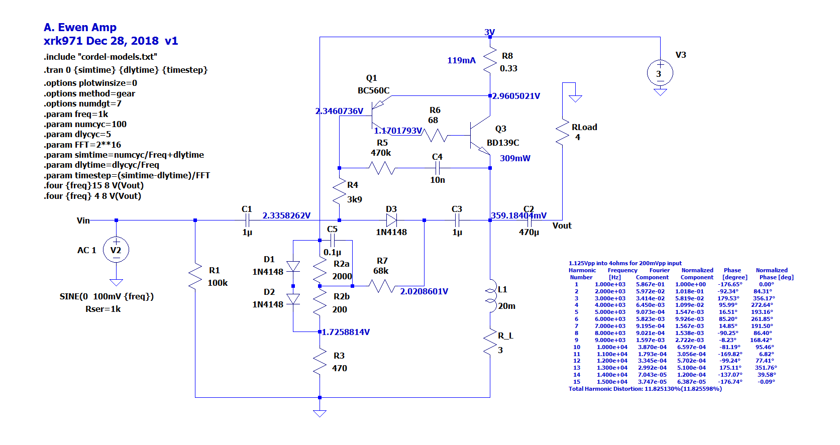
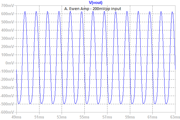
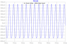
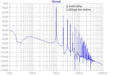
Perhaps I am not doing something right but I tweaked 2k2 pot to almost bottom of travel to get sufficient bias current. Amp has interesting property that high impedance load will give a quasi square wave output, that is distortion goes up with decreasing impedance! At 4R, it has about 12% THD and FFT looks like quite a mess. Hmm... is something off here? Playing with value of inductor had no effect on distortion. I connected load to GND, and connected as shown originally had same output. There was no benefit of connecting speaker to a hot battery lead other than potential for sparks and fire.
Schematic:
Simulated Oscope for 4ohm load:
FFT for 4ohm load:

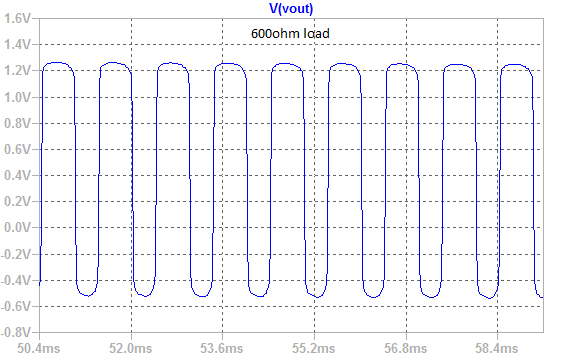
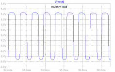
Here is 600ohm load:
Schematic:
Simulated Oscope for 4ohm load:
FFT for 4ohm load:
Here is 600ohm load:
Attachments

Last edited:
How about trying it with the specified diodes - 1N4002.Perhaps I am not doing something right but I tweaked 2k2 pot to almost bottom of travel to get sufficient bias current....
Greetings.
Just looked through the post and diagram, and yes, no value.
It measured 33mH, if that's of any help.
The bias pot only sets idle current, 20 - 25mA is good. The adaptive feedback bias that makes this interesting sent all of my attempts at simulation cattywhumpus. A bigger op transistor is a must for experimentation.
Its perhaps something that convetion dictates shouldn't work well, but does, (with the caveat that it wouldn't impress an audiophile if you touted it as Hi Fi).
Regards,
Norman.

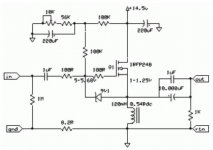
Looks i did something wrong in post #7.The missing part
Mona
This fails 2 of the initial requirements:
1. Power supply 3v.
2. Adaptive bias to minimise power consumption.
I doubt that the type of diode changes anything as long as it is a silicon diode. I put 1N4004 (higher voltage version on 1N4002), Made inductor 35mH, set bias to 25mA and still get a similar behavior.
Code:
Harmonic	Frequency	 Fourier 	Normalized	 Phase  	Normalized
 Number 	  [Hz]   	Component	 Component	[degree]	Phase [deg]
    1   	1.000e+03	5.465e-01	1.000e+00	 -177.98°	    0.00°
    2   	2.000e+03	6.175e-02	1.130e-01	  -91.14°	   86.84°
    3   	3.000e+03	2.076e-02	3.799e-02	  177.69°	  355.67°
    4   	4.000e+03	5.712e-03	1.045e-02	   83.99°	  261.97°
    5   	5.000e+03	2.349e-04	4.298e-04	  -52.07°	  125.91°
    6   	6.000e+03	1.451e-03	2.655e-03	   86.04°	  264.02°
    7   	7.000e+03	1.204e-03	2.204e-03	   -9.08°	  168.90°
    8   	8.000e+03	4.297e-04	7.862e-04	 -107.17°	   70.81°
    9   	9.000e+03	1.447e-04	2.648e-04	    7.75°	  185.73°
   10   	1.000e+04	2.874e-04	5.260e-04	  -98.95°	   79.03°
   11   	1.100e+04	1.691e-04	3.094e-04	  163.54°	  341.52°
   12   	1.200e+04	2.107e-05	3.855e-05	    4.40°	  182.38°
   13   	1.300e+04	7.106e-05	1.300e-04	  177.02°	  355.00°
   14   	1.400e+04	5.702e-05	1.043e-04	   75.11°	  253.09°
   15   	1.500e+04	1.708e-05	3.126e-05	  -50.00°	  127.97°
Total Harmonic Distortion: 11.972628%(11.974771%)I will copy the assignment here for better appreciation of the challenges involved.
Getting decent radio receiver performance out of a single transistor is no mean feat but doable if you know about reflex (as used here) and regenerative circuits. That leaves 2 transistors for the audio amp. Still tough on 3 V.
xrk's simulation results look plausible... gain is going to be approximately Rload / 0R33 (so you'd need to dial down input amplitude or increase degeneration for higher-impedance loads), and bias needs to accomodate one diode at low current plus one B-E drop and change from B+, so its setting being near the low end makes sense. I imagine using a germanium or Schottky diode may give better results, as it typically does in AM detectors... which is pretty much what this autobias circuit is after all. I would also prefer attenuating diode detector output between the diode and the 3k9 instead of making the coupling capacitor as small as it is.
As for distortion, at these low voltages saturation becomes very important, which is going to vary a fair bit depending on transistor type, not to mention potential modelling inaccuracies. I'd double-check with something like 1N5087 and BC337 models. In general, the less complex a circuit, the more it is susceptible to component variation.
Just for reference, it would be interesting to know how the load inductor holds up at load current. Pretty well, I'd assume, given it appears to be gapped and decent large.
My first reaction would be: "3 transistors? What year is this, 1965?" I think the last people to face a challenge like this were (budget) transistor radio designers right around that time. (And even then, they'd have preferred the trusty 9 V block battery.) I mean, I admire minimalist but functional designs as much as the next guy, but there's a limit to everything.The term practical work project is to research and build a design for a functional radio receiver, the requirement for the completed set is that it can resolve local stations transmitting on the medium wave band with good selectivity and clarity, the test of sensitivity will be its ability to receive a 1KW station on 648KHz that is 100Km distant without any external antenna The design can be original or preexistent but the student must have built it and be able to demonstrate understanding of its function.
The technical specifications of the receiver are that it:
1. Should be transportable and self contained.
2. Be powered by primary cells, at a nominal maximum of 3volts.
3. Will include no more than 3 active devices. They will be bipolar transistors, and can be selected from types BC327, BC337, BC549, BC559, in any combination.
4. Will drive a loudspeaker so it can be used by multiple listeners.
5. Incorporate in its design an automatic method by which its battery power consumption is demonstrably economised, at low sound volume.
Marking will be by grade average and will be judged by:
6. Sensitivity.
7. Selectivity, its ability to separate signals.
8. Sound quality.
9. Maximum achievable sound level meter results before the onset of output clipping.
10. Economy, cost of battery cell's divided by hours running time, at a specific "volume" (Extrapolated from consumption and manufacturer data on cells capacity).
Getting decent radio receiver performance out of a single transistor is no mean feat but doable if you know about reflex (as used here) and regenerative circuits. That leaves 2 transistors for the audio amp. Still tough on 3 V.
xrk's simulation results look plausible... gain is going to be approximately Rload / 0R33 (so you'd need to dial down input amplitude or increase degeneration for higher-impedance loads), and bias needs to accomodate one diode at low current plus one B-E drop and change from B+, so its setting being near the low end makes sense. I imagine using a germanium or Schottky diode may give better results, as it typically does in AM detectors... which is pretty much what this autobias circuit is after all. I would also prefer attenuating diode detector output between the diode and the 3k9 instead of making the coupling capacitor as small as it is.
As for distortion, at these low voltages saturation becomes very important, which is going to vary a fair bit depending on transistor type, not to mention potential modelling inaccuracies. I'd double-check with something like 1N5087 and BC337 models. In general, the less complex a circuit, the more it is susceptible to component variation.
Just for reference, it would be interesting to know how the load inductor holds up at load current. Pretty well, I'd assume, given it appears to be gapped and decent large.
Using an inductor as a load element allows the output to swing beyond the supply rail; in this case, the bottom rail. That may be important in a 3V-only amplifier.
Watch out that you don't exceed the "Vebo" maximum rating for emitter-to-base reverse bias of the NPN transistor, when the output signal swings to its maximum.
Watch out that you don't exceed the "Vebo" maximum rating for emitter-to-base reverse bias of the NPN transistor, when the output signal swings to its maximum.
Greetings.
Nailed it sir!
We used the method in the early transistor car radio output stages to save on one transistor (more expensive than the choke) and theoretically gain extra output.
Wouldn't make commercial sense now, but a good foil for that restrictive (thought provoking?) project.
One question, why would the output transistor BE junction become reverse biased?
Regards,
Norman.
Using an inductor as a load element allows the output to swing beyond the supply rail; in this case, the bottom rail. That may be important in a 3V-only amplifier.
Nailed it sir!
We used the method in the early transistor car radio output stages to save on one transistor (more expensive than the choke) and theoretically gain extra output.
Wouldn't make commercial sense now, but a good foil for that restrictive (thought provoking?) project.
One question, why would the output transistor BE junction become reverse biased?
Regards,
Norman.
Greetings.
Original testing, (on my build of the circuit) with a resistive load (sweeping 100Hz to 100KHz at 5s sweep) showed flat within 3db then rolling off above 7KHz, (AM radio, so who cares?.) with no parasitics IIRC.
THD+noise was remeasured, longhand, with filters. It's not at all bad for an SE amp at 3.23% but done with the caveat the student specified in her post, ie. Not being possible to load the amplifier to clipping with the transistors available for the project, re their survival.
Transient distortion on step changes of input level were bad in that they could be seen on an oscilloscope, although difficult for a non golden ear to hear. (I don't buy green bananas anymore).
I tried to upload pictures of the spectrum sweep, but wasn't able, the tablet I'm using is refusing to let me upload the jpeg file (pop up not responding).
My opinion is reinforced that, if it works in simulation, it'll work in hardware. But if the hardware works, don't necessarily expect it to simulate.
Thanks,
Norman.
- Status
- This old topic is closed. If you want to reopen this topic, contact a moderator using the "Report Post" button.
- Home
- Amplifiers
- Solid State
- simple adaptive bias bipolar amp