I am sure that this will be of interest for many of you.
Recently the German mag "ImageHiFi" (4/2005) did a favorable review of the Shigaraki CDDrive and DAC. The wrote "... the Shigaraki system eats many other very expensive CD Players for breakfast..."
I hope I do not break any copyright rules by posting excerpts of the images, if yes, please do not tell them 🙂
In the article were a few interesting inside shots of the PSU and the DAC.
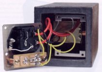
First the PSU opened:
Now everybody can see clearly that they use half-wave rectifying (like NAIM, and like I have always proposed...), that means two secondaries with two diodes only for a single output voltage. The diodes seem to be the already mentioned General Semiconductor FE5B (or C), 5Amps rated. Considered the size of the DAC including the ceramic case (7,6 x 7,6 x 14 cm), the transformer is quite small.
Recently the German mag "ImageHiFi" (4/2005) did a favorable review of the Shigaraki CDDrive and DAC. The wrote "... the Shigaraki system eats many other very expensive CD Players for breakfast..."
I hope I do not break any copyright rules by posting excerpts of the images, if yes, please do not tell them 🙂
In the article were a few interesting inside shots of the PSU and the DAC.
First the PSU opened:
Now everybody can see clearly that they use half-wave rectifying (like NAIM, and like I have always proposed...), that means two secondaries with two diodes only for a single output voltage. The diodes seem to be the already mentioned General Semiconductor FE5B (or C), 5Amps rated. Considered the size of the DAC including the ceramic case (7,6 x 7,6 x 14 cm), the transformer is quite small.
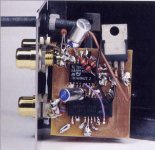
Second the DAC opened:
Here the image does not reveal the complete secret, but a lot of details nevertheless. The pcb looks very much "47labs-style", a bit DIY too much, considered to the efforts of some of you here. It is a mixture of p2p and pcb, it has to be like that, I think, although some details (the blue wire!) looks like an afterthought.
The DAC uses a single regulator (a 7805 perhaps), smoothing caps are either non-existent or not visible. SPDIF input (with a carbon 75R resistor) goes into a CS8414 directly. The pll filter uses an elcap (or is it the smoothing cap for the digital supply side?). The ShagirakiDAC uses a TDA1543 not in the DIP8 case, but in the 16minipack smd size, recognizable by the 8 "outside" feet soldered together, although the exact number on the chipcase is not fully readable. Maybe the heat dissipation of this package is better the smaller DIP8 chip. Two 3k carbon resistors are soldered on top of the TDA, maybe the IV conversion resistors. Another stripped cap is visible, maybe one of the output caps.
That is more or less what I can see. Now it is up to you for conclusions and further analysis.
Attachments
lohk said:...Now everybody can see clearly that they use half-wave rectifying...that means two secondaries with two diodes only for a single output voltage.....
It's a full wave rectifier then, don't you think?
Looks pretty ugly to me, both visually and design wise...I hope they aren't charging much for that thing, but something tells me they are 
Actually this arrangement of rectifiers could be expected, as it also appears in Kusunoki DACs. The rumour is that 47Labs pay royalties to Kusunoki for using non oversampling concept, that could be one reason the price of the DAC is so high.
I guess it doesn't give us that more info then we allready have.
Except for one side of the lay-out. Pretty important.
Except for one side of the lay-out. Pretty important.
lohk said:Second the DAC opened:
SPDIF input (with a carbon 75R resistor) goes into a CS8414 directly.
There could be capacitors on the other side?
The pll filter uses an elcap (or is it the smoothing cap for the digital supply side?).
How do you recognise which one is the pll filter?
Ha, sure there must be caps on the other side 
and the cap can be for any of the mentioned purposes, its an elcap.
I should not have wasted my precious time in scanning the images and post them to this forum, you have known all facts anyway.
and the cap can be for any of the mentioned purposes, its an elcap.
I should not have wasted my precious time in scanning the images and post them to this forum, you have known all facts anyway.
Although I've heard what's inside Shigaraki DAC 2 years ago, a picture is worth a thousand words 😉
The supply voltage to DAC was said to be 8V.
The supply voltage to DAC was said to be 8V.
lohk said:Ha, sure there must be caps on the other side
and the cap can be for any of the mentioned purposes, its an elcap.
Eehm, u don't think there are caps on the other side? Correct me if I'm wrong, I'm not really familiar with Englisch/American forum-slang 😀

There must be a second regulator then, somewhere hidden inside the DAC (on the dark side of the pcb), or does the CS8414 tolerate 8V (maybe a smaller one or a TL431)?
Those are the caps I meant, thanks. The previous poster did me believe that he thought there weren't any caps there. But I must have misunderstood.
The other regulator is on the other side, must be 😉
The other regulator is on the other side, must be 😉
If I see correctly, they use a cable between SDATA and DATA. I thought this was one of the most important connections since the digital data is led through there. then why a cable and no hardwire between the pins? Am I wrong? They chose to wire FSYNC and SCK as short as possible. Can anyone think of a reason? Why are they so important? I can read in the datasheet what the pins do but don't quite understand it.
It seems to be a single side pcb, only the SDATA (pin26) - DATA (pin5) connection is on the "wrong" side of the receiver chip. Maybe the blue wire is then the shortest path. The other connections have only a short path on the pcb.
Bit clock and word select connections are surely as important. Without a correct information here the data stream is worthless, I think.
You understand by my words that my knowledge and experience about all that is restricted.
(I only think that the PeterDaniels pcb has a shorter path still..)
You understand by my words that my knowledge and experience about all that is restricted.
(I only think that the PeterDaniels pcb has a shorter path still..)
Thank you.
Has anyover ever experimented with hardwiring the SDATA against hardwiring FSYNCK and SCK?
And does it matter if I bend the pins on the chips? Sure, I shouldn't do it to much since the metal will break, but if it doesn't? Will I lose quality or is it just smart configuring? 😉
Has anyover ever experimented with hardwiring the SDATA against hardwiring FSYNCK and SCK?
And does it matter if I bend the pins on the chips? Sure, I shouldn't do it to much since the metal will break, but if it doesn't? Will I lose quality or is it just smart configuring? 😉
- Status
- Not open for further replies.
- Home
- Source & Line
- Digital Source
- Shigaraki Drive and DAC images