Wavebourn,
I also attached a THD vs Power graph I made of my mono LME49811 based Amplifier with 50VDC rails into an 8-ohm load.
I would love to try these new FET devices with the LME49830 boards and compare them (listen and test) with the LME49811 based power amps I have. Benchtester and I should have the 811 based amps on display at Burningamp!
Best Regards,
Mark / Audioman54
811? Is that 811 tubes or 811 ICs??
And no attachment seemed to be visible...
_-_-bear
Looking at the data sheet they spec quite low resistance for the gate and quite high gate current.
When I look at the curves, it looks like about 1 uA at 5 amps
Ids, and it does go up to 10 uA at 10 amps Ids or so. I
consider this low enough to not be an issue.
811? Is that 811 tubes or 811 ICs??
National often re-uses famous numbers, don't know why. For example, NJR parts 4562 were commonly used in an audio pro-gear...
Like ICBMs.
I wonder, if it is possible to import Russian missiles for audio parts. Some of them were destroyed according to Gorbachov's weapon reduction plan, but what happened to electronics from them? 🙄
I wonder, if it is possible to import Russian missiles for audio parts. Some of them were destroyed according to Gorbachov's weapon reduction plan, but what happened to electronics from them? 🙄
I'd search in the Baltic's if such parts were needed 😉
Magura 🙂
I'd search in the Baltic's if such parts were needed 😉
It is exactly where I bought a box of MLT resistors, though number of nominals is very limited. 🙄
<<Ive been looking into these SIC devices and found a company producing them in Japan, they have quite a range. At the moment Im trying to get datasheets pricing and availibity on them then Ill post some info. Preliminary pricing seems to be around $15 for a 20 A device.>>
Since Homemodder is working on this, I wonder if anybody have tried to follow the lead on the real SIT:
http://www.diyaudio.com/forums/showthread.php?t=124730
I have posted that info with the belief, that those, who are interested will notice.
Since Homemodder is working on this, I wonder if anybody have tried to follow the lead on the real SIT:
http://www.diyaudio.com/forums/showthread.php?t=124730
I have posted that info with the belief, that those, who are interested will notice.
In a previous life I was looking at SiC for image sensors and high power microwave devices.
In my present life I make RF amplifiers in the 100 MHz to 1 GHz region. CREE makes SiC devices for RF power amplifier use up to 2.7 GHz. We evaluated the early production devices about 3 or 4 years ago. Like many RF devices made for operation in the 2 GHz + region they have too much gain at 136 MHz and tend to be unstable. They often oscillate and blow up. The Ultra RF (now part of CREE) rep got us a couple of the pre production devices, and yes we blew them up. These parts make the SemiSouth parts look cheap. They are about $500 each!
I have been experimenting with a hybrid tube - mosfet (or bipolar) "darlington" configuration. This provides vacuum tube curves at 1 amp + "plate" currents. The SiC parts may make a good match here.
Member
Joined 2009
Paid Member
In my present life I make RF amplifiers in the 100 MHz to 1 GHz region. CREE makes SiC devices for RF power amplifier use up to 2.7 GHz. We evaluated the early production devices about 3 or 4 years ago. Like many RF devices made for operation in the 2 GHz + region they have too much gain at 136 MHz and tend to be unstable. They often oscillate and blow up. The Ultra RF (now part of CREE) rep got us a couple of the pre production devices, and yes we blew them up. These parts make the SemiSouth parts look cheap. They are about $500 each!
I remember Cree, came out of Carolina University ?
I have been experimenting with a hybrid tube - mosfet (or bipolar) "darlington" configuration. This provides vacuum tube curves at 1 amp + "plate" currents. The SiC parts may make a good match here.
One of my favourite compound devices is the CFP. I can imagine using a tube for the master and a SS device for the slave. I have been looking at low voltage tubes for this though - I have access to some nuvistors that run with a heater current of only 130mA...
When I look at the curves, it looks like about 1 uA at 5 amps
Ids, and it does go up to 10 uA at 10 amps Ids or so. I
consider this low enough to not be an issue.
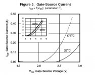
I was looking at for instance Fig 5 in the data sheet. This must be an error, no?
If not, it looks like you really need significant gate current for high Id currents.
jd
Attachments
Last edited:
Exactly janneman, I was wondering that too 😕 Let me try to suggest some ideas. Aren't we talking about a JFET like device? Isn't the fig. 5 only showing positive G-S? Are we not more interested in neg G-S? If you were to extrapolate those curves down to 0V G-S would you not be in the area more typical devices Ig (Idss)? The threshold is stated to be approx. 1V. Isn't that -1V 
It is very typical for engineering to provide the data for datasheets but by the time the document group (not technical enough) is done editing it, will be messed up!
It is very typical for engineering to provide the data for datasheets but by the time the document group (not technical enough) is done editing it, will be messed up!
Exactly janneman, I was wondering that too 😕 Let me try to suggest some ideas. Aren't we talking about a JFET like device? Isn't the fig. 5 only showing positive G-S? Are we not more interested in neg G-S? If you were to extrapolate those curves down to 0V G-S would you not be in the area more typical devices Ig (Idss)? The threshold is stated to be approx. 1V. Isn't that -1V
It is very typical for engineering to provide the data for datasheets but by the time the document group (not technical enough) is done editing it, will be messed up!
I don't know, from what I understand from Nelson is that you can get up to say 10A Id with very low Ig (at Vgs below 2V or so) but that grapgh doesn't show those lower values.
I don't want to make an issue here, just wondering.
jd
They did not provide the normal Idss type curve in those datasheets? I think that is one of the important parameters for our use. When you go much beyond 0Vgs in the positive direction you start seeing a diode forward drop and associated non linear current. Driving the gate negative begins controling the device the way we normally do until pinchoff 😀
That's what I'm expecting for a JFET type device at least ???
That's what I'm expecting for a JFET type device at least ???
They did not provide the normal Idss type curve in those datasheets? I think that is one of the important parameters for our use. When you go much beyond 0Vgs in the positive direction you start seeing a diode forward drop and associated non linear current. Driving the gate negative begins controling the device the way we normally do until pinchoff 😀
That's what I'm expecting for a JFET type device at least ???
It's a normally-off device so you make the Vgs positive until conduction starts around a volt or so. Nothing unusual. What I do find unusual is that when you start to go above 2V Vgs or so, appreciable gate current starts to flow. Maybe it is good for audio, kind of automagically limit Id to safe values?🙂
For instance, for Id=12A you need 3V Vgs and the typical Ig is then 300mA. Bit hefty, no?
jd
Last edited:
Let's study the datasheet (staying with ...R125).
Fig4: Vth~1V (even with low resolution/big scale). To bias to ~3A we will need ~1.4V Vgs. That will leave us with only ~0.4V signal Negative amplitude to stay in class A. With the signal Positive peak the Vgs will rise to~1.8V. (Pretty high sensitivity due to high Gm).
Fig5: Ig starts at ~2.4V Vgs, at 25degC, (we can say even ~2.3V, or so, due to the chart low resolution). Even at 175degC that voltage is 2-2.1V. Since we are limited to Vgs max 1.8V, gate will not start to conduct any significant current.
I will also mention, that the thermostable current for THIS part# is just below 3A.
Fig1, T=25 deg: at Vgs=1.5V Id~3.5A.
Fig2, T=125 deg: at Vgs=1.5V Id~3.0A.
Fig3, T=175 deg: at Vgs=1.5V Id<3A
So, if we start at 3.5A, the Id current tempco is already negative.
😎 Thanks StevenOH. That seems to coincide with some statements N.P. made back at the first page...
😉
😉
Is the model no. SJEP120R100 (the 17A) version same or better to use in place of the discontinued R125 (15A) part?
(also because I have found a good price 😉 )
(also because I have found a good price 😉 )
Is the model no. SJEP120R100 (the 17A) version same or better to use in place of the discontinued R125 (15A) part?
(also because I have found a good price 😉 )
Telstar, from the information I have received from then, the 100 is the replacement, just so that's clear.
These SiC JFETs definitely look interesting. If/when I get some, I have a preliminary design I'd like to try.
Preliminary Schemo
Class A
Vdd= 300Vdc
Vo= 150Vp / phase
Po= 50W
Rl= 900R (D-2-D)
Ip= 0.33A
Idq= 0.367A
Pd= 110W / phase
The A Number One problem is that these are definitely high voltage devices, as seen from the capacitance plot: Capacitance. At the more usual SS voltages (<100V) the capacitances go almost vertical. That's not good at all.
Running at 300Vdc helps improve that considerably, and 600V would be even better. However, that demands an OPT to protect the end user from some serious voltages. That leaves out any sort of OTL topology.
For the front end, these small signal, depletion type MOSFETs (DN3545 -- Supertex) look pretty good here. Since these have some rather high Ci's, cascode them to eliminate the Cmiller problem.
Possible optimizations: Include drain-to-gate NFB on the input LTP cascodes to improve linearity, and to get the gain down, as it just might be excessive here. May also need source follower gate drivers since these JFETs have quite a bit more Ci than you'd find in a comparable hollow state design.
Definitely something to try out when RL stops interfering.
- Status
- Not open for further replies.
- Home
- Amplifiers
- Solid State
- SemiSouth SiC Power JFETs