ostripper said:
too many freeekin' diodes..maybe a couple white LED's 😀
OS
Yes, there are leds also, see note beside schematic.
Sparcnut, if Im not mistaken thats the inputstage of nationals lm6172 series opamp, very high slewrate, I used to have a diagram of it but its lost somewhere between all my harddrives till I can locate it again.
homemodder said:Sparcnut, if Im not mistaken thats the inputstage of nationals lm6172 series opamp, very high slewrate, I used to have a diagram of it but its lost somewhere between all my harddrives till I can locate it again.
Yes, it essentially is. They show a simplified schematic in their datasheet, but make it not obvious that they use two identical diamond buffers for the inputs. There's a Linear Tech part that uses the same stage as well - the LT1361. Their schematic is much more detailed. I think they both got the idea from the Smith paper.
My implementation is different because of the output stage and its biasing. I also use individual degen resistors to bridge the two input buffers to control the idle current, which I suppose wouldn't be necessary on an IC with good thermal tracking.
I cant remember the exact circuit, I ll have to find my notes on my hardrives but I was keen to try something like that for a poweramp but decided against it because complexity and possible stability issues, however the lm6172 is a mighty good sounding opamp but a lot of care must be taken with layout and bypassing. I might just be inspired to try something like this, whats the sound like compaired to other circuits. Anything it does better subjectively ???
The performance specs you state, are those with those awfull 2n parts???
Ill take a look at the lt part, wasnt aware of this one.
The performance specs you state, are those with those awfull 2n parts???
Ill take a look at the lt part, wasnt aware of this one.
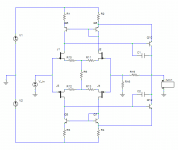
For a simpler class AB input stage, JFETs can be used, as per the attached schematic. There isn't actually any need for the current mirrors here, so plain resistive loading can be used instead if desired.
Using JFETs gives a far simpler circuit, but ends up more expensive. R5 really needs to be variable to allow for the large variation in Idss between devices (you couldn't get away with sparcnut's version where R5=0 unless you don't care what the quiescent current is).
Using JFETs gives a far simpler circuit, but ends up more expensive. R5 really needs to be variable to allow for the large variation in Idss between devices (you couldn't get away with sparcnut's version where R5=0 unless you don't care what the quiescent current is).
Attachments
It's just the standard complementary JFET LTP, which I think most people fail to notice is actually class AB. I used it in my subwoofer amplifier. I would use it more, but I'm loathe to deplete my precious stock of 2SK389/2SJ109.Wavebourn said:Inspired by John Curl?
homemodder said:I cant remember the exact circuit, I ll have to find my notes on my hardrives but I was keen to try something like that for a poweramp but decided against it because complexity and possible stability issues, however the lm6172 is a mighty good sounding opamp but a lot of care must be taken with layout and bypassing. I might just be inspired to try something like this, whats the sound like compaired to other circuits. Anything it does better subjectively ???
The sound is completely neutral. There's quite literally nothing to hear, it is essentially the famed "straight wire with gain". It is the only output stage I have heard that gets cymbals completely correct, I suspect the absence of IMD products at high frequencies is the main reason. My headphone amp uses this as an output stage, driven by THS4032 chips doing the signal processing (multichannel mix, linkwitz transform, crossfeed).
Using this topology in a power amp is maybe not advisable, my headphone version was very touchy until I figured out how to keep the high frequency stuff under control. Closing a feedback loop with gain out to 35MHz on a perfboard is not simple, it seems. 😀
The main competitor I had to this design was the THS6012 ADSL driver chip on a custom carrier board, which does perform quite well (see here). But the discrete circuit still kills it in distortion performance (see here). (Measurements are with a notch filter, so imagine a 1khz fundamental at 0dbV). The subjective difference between the two is a slightly cleaner high end on the discrete circuit. Cymbals make a clean PSSSSSSS sound, not PSHSSHSHSSSHS.
One detail I did not show in the schematic is the output RLC network. This is important for stability. I have attached a slightly better schematic that includes it. The 33nH inductor is a small generic ferrite bead; the 33nH value is very approximate. The intended load is the ATH-A700/A900, so the load impedance is expected to be 64 or 40 ohms with ~102dB/mW sensitivity. You can go higher, just watch out for the signal swing - stay at least 5v or so from the rails for best linearity.
I'm not sure what's particularly awful about them, but yes, those specs are measured with the devices shown. I used completely unmatched devices from a single batch of Farchild parts. As I mentioned earlier, the only parts I used that are different from the schematic are the output MOSFETs; I used BS170/BS250 instead of the Zetex fets. I don't think the substitution makes much difference - they're all common vertical switching fets. The Zetex complementary fets may even match somewhat better. None of the fets are exactly cheap compared to the 3904/3906 bipolars ($0.04 vs. $0.25-$1.50 each), but the whole board still cost me under $20.The performance specs you state, are those with those awfull 2n parts???
I have a few more AP plots of it here. These tests are at unity gain, 1v into 50 ohms ("typical" level on the ATH-A700s is actually more like 100mV so this is worst-case). You can see that THD-1K is about -117dB, THD-10K is about -106dB, IMD-10K+500 is about -106.
And of course, some obligatory pictures of the actual prototype: top, bottom. The TL082 is the DC servo. The soldering may look a little excessive, but keep in mind this is a pad-per-hole board so I connect adjacent pins by bridging, which requires a large blob.
Attachments
Mr Evil,
it is of course possible to reduce complexity to a minimum but then you will have to live with its consequences. Why on earth would anyone want to class AB bias an input stage? Your theories and ideas indicate a big confusion so you should stick with readily available designs as you most unlikely can come up with something better.
it is of course possible to reduce complexity to a minimum but then you will have to live with its consequences. Why on earth would anyone want to class AB bias an input stage? Your theories and ideas indicate a big confusion so you should stick with readily available designs as you most unlikely can come up with something better.
The point of class AB input stages is to increase their current capability without increasing their quiescent current, and like I said, this gives you increased slew rate.Lumba Ogir said:...Why on earth would anyone want to class AB bias an input stage?...
Why would you want increased slew rate? Mostly it's just an academic exercise, the same as decreasing distortion to extremely low levels, or having very high damping factor, but we always seek to improve the specs. More specific reasons might be ensuring that TIM cannot occur, or reducing quiescent current for lower power consumption for a battery operated amp.
I'm not sure why you've decided to start insulting me. Have I offended you somehow?Lumba Ogir said:...Your theories and ideas indicate a big confusion so you should stick with readily available designs as you most unlikely can come up with something better.
Mr Evil,
you have not offended me in any way but the numerous theoretical and practical flaws in your presentation disturb me greatly.
you have not offended me in any way but the numerous theoretical and practical flaws in your presentation disturb me greatly.
Wavebourn,
not having your native sense and intuition, I certainly could not have been able to spontaneously cook up such a solution.
not having your native sense and intuition, I certainly could not have been able to spontaneously cook up such a solution.
Lumba Ogir said:Wavebourn,
not having your native sense and intuition, I certainly could not have been able to spontaneously cook up such a solution.
It is easy: throw all available parts and information in subconscious mind, forget, and wait until it's fully cooked. That's it.
Meditation helps to train cooking abilities.
Hi sparcnut -
Did you consider or try BJTs in your output stage? What advantage do MOSFETs have over a BJT diamond buffer output stage?
Did you consider or try BJTs in your output stage? What advantage do MOSFETs have over a BJT diamond buffer output stage?
RDS-on might get you closer to either rail than VCE-sat?
Simplified thermal stability? Reduced drive current?
Nothing important...
Simplified thermal stability? Reduced drive current?
Nothing important...
nuvistor said:Hi sparcnut -
Did you consider or try BJTs in your output stage? What advantage do MOSFETs have over a BJT diamond buffer output stage?
The first version of it I built had a BJT diamond buffer output stage. The MOSFET version I designed and built later, which is what you see here, has lower distortion and higher speed.
Bipolar diamond buffer version, MOSFET version. Check out the nasty set of high-order odd harmonics. The difference is -100dB versus -117dB, not a small one at all IMO. Those last few dBs are the hardest to get!
It is worth noting that the MOSFET version pulls 0.0004% THD+N, unweighted, 20Hz-20KHz. The "sweet spot" where THD+N is minimized for a 50 ohm load is from 1v to 3v of output.
kenpeter said:RDS-on might get you closer to either rail than VCE-sat?
Simplified thermal stability? Reduced drive current?
Nothing important...
I wouldn't call any of those things unimportant.
The gains I noted going to fets from the bjt diamond were:
* More usable GBP for the entire amplifier. This is because the faster output stage allowed the degen resistors in the input stage to go down from 47R to 22R, which adds about 6dB open-loop gain (and feedback) at all frequencies and pushes the unity gain bandwidth out further - from ~15MHz to 35MHz when set for 60 degrees phase margin.
* Much lower distortion. Maybe the base charge in the bjt version is not being removed quick enough? I tried using various methods to remove the base charge faster and came up with no clear improvement. This isn't the usual crossover distortion, there is a good 1-2mA idle current flowing through every output BJT; they just stick for a few nS when asked to turn off I think. I remember looking at the drive waveform on a 'scope and seeing a huge (0.5v?) spike when crossover occurs in either direction.
* Much higher slew rate: 1000V/uS instead of 450V/uS. Probably due to lower degen resistors in input stage, those plus the capacitance at the output of the current mirror determine the maximum slew rate.
* Simpler compensation (fets' internal Cgd totals 100-200pF, no external caps needed)
* Easier to drive. A big issue with the bjt output was turning output bjts on hard enough to get lots of output current in a linear way. The high driver idle current required for this ends up being wasted in the drivers when it's not needed. The drivers themselves then become nonlinear and hot. Darlingtons were not an option because they turn off far too slowly; CFPs were not an option because they were just plain unstable when combined with the ludicrously fast frontend. The LM6171 "solves" this problem by using the slew current to control the driver bias (look at the extra mirror output in their schematic), but this only works for relatively low output currents (under 20mA or so). Beyond that, huge multiplying factors are needed, and here comes the nonlinearity and heat again.
The main downside to the fets is that they can't drive as close to the rails, since Vth >> Vbe and the slope of the Vgs vs. Id curve is << than the Vbe vs. Ic curve. That's not an issue in my application though.
Regarding cfb2.pdf
If you abused simple bootstraps rather than BJT current mirrors,
you could swing necessary drives for rail to rail output no probs.
Also not sure why you diamond buffered the output backwards?
Rather than compare centerpoint Q3 Q4 to the output directly?
Your output impedance is plenty low enough to handle it.
Thanks for the detailed reply!
How good is output stage thermal stability? I see you're using a Vgs multiplier.
Your schematic shows a closed loop gain of 1, have you tried higher CLGs, perhaps 3 to 5?
I would have expected the higher BJT transconductance to result in lower distortion, but the proof is in the testing. Perhaps a diamond buffer loads the VAS more at audio frequencies than the small MOSFETS?
BJTs have storage time so turnoff is not immediate, MOSFETs turn off as soon as gate charge is removed. I would not expect this to be a problem with the limited slew rate of audio signals and small-signal BJTs.
To be honest I can't say I have been impressed by your theoretical and practical level either, especially given your peculiar assertions in the ceramic capacitor thread, but if you actually know something that isn't uselessly vague, then I am always eager to learn.Lumba Ogir said:Mr Evil,
you have not offended me in any way but the numerous theoretical and practical flaws in your presentation disturb me greatly.
- Status
- Not open for further replies.
- Home
- Amplifiers
- Solid State
- Self-biasing class AB input stage