Hello all,
I'm working on rebuilding a Kenwood KA-9100 integrated amp and the need has come to replace the input differential pair JFETS (Qi 21 and 23) in the phono section. The original were 2sk68a L rank parts. The replacement parts I received are N rank parts with different Vgs on / off and IDSS parameters. I thought it would still be possible to use these new parts with some reconfiguration of the source and drain resistors in the circuit. I will present my math and reasoning below and I'm hoping that someone more knowledgeable than I would be willing to check my math and reasoning.
The original Jfet had the parameters Vgs OFF: - .45V Vgs ON: 0.22V IDSS: 2.2 mA
Current through the drain resistors (RI 105, 107) is 16.5V / 22K = 0.75 mA each
voltage drop across source resistor (Ri 109) is 1.5 mA * 10K = 15 V
Current through Ri 113 is 14.1 V / 3.3k =4.27 mA
Current through Ri 111 is approximately 4.27 mA - 1.5 mA = 2.77 mA
The new JFET parameters are Vgs OFF: -.8V Vgs ON: -0.1V IDSS 5.5 mA
For the new circuit, I will maintain the drain voltage of 11.5 V for proper biasing of the downstream stage. I am planning on using a source voltage of 350 mV (about 50% of the difference between Vgs on and off). I am planning to use a drain current of 2.5 mA (nominally around 50% of the IDSS).
New drain resistor values for RI 105 and 107 is 16.5V / 2.5 mA = 6.6 Kohm each
For calculating the source resistor i need to take into account the increased voltage drop through Ri 113 due to the increased current as this will lower the available voltage at the junction of Ri 109, 111, and 113. I used a bit of a guess and check method here instead of setting up a system of linear equations because I am not fresh out of school at this point. I know I need 5 mA through the source resistor Ri 109 so I know that the current through Ri 113 must be greater than that to allow current to flow to ground through Ri 113 (at least I think that is the correct assumption). In this case I assumed a current of 6.5 mA through Ri 113
Thus the voltage at the Ri 109, 111, 113 junction is 6.5 mA * 3.3k = 21.45 V, 29V-21.45 = 7.55 V
Thus the new source resistor voltage drop is 7.55 V + .35V (source voltage) = 7.9 V and thus the new source resistor value is 7.9 V / 5 mA = 1580 ohms
I'm hoping that the voltage divider with ri 111 isn't critical for some reason that Im unaware of and is ok with the reduced current through it compared to the original
design. The math is simple enough I hope but I really need help with checking the assumptions I used. Hopefully the new values I came up with would work better than leaving the stock values!
2SK68A (L): Vpo = -0.45, Idss = 2.2mA... what do you specify with the "ON: 0.22V"?The original Jfet had the parameters Vgs OFF: - .45V Vgs ON: 0.22V IDSS: 2.2 mA
...
The new JFET parameters are Vgs OFF: -.8V Vgs ON: -0.1V IDSS 5.5 mA
unknown jF: Vpo = -0.80, Idss = 5.5mA... what do you specify with the "ON: -0.1V"?
Why?... and the need has come to replace...
Calculations are ok.Current through the drain resistors (RI 105, 107) is 16.5V / 22K = 0.75 mA each
voltage drop across source resistor (Ri 109) is 1.5 mA * 10K = 15 V
Current through Ri 113 is 14.1 V / 3.3k =4.27 mA
Current through Ri 111 is approximately 4.27 mA - 1.5 mA = 2.77 mA
You have to maintain that Vds indeed.For the new circuit, I will maintain the drain voltage of 11.5 V for proper biasing of the downstream stage. I am planning on using a source voltage of 350 mV (about 50% of the difference between Vgs on and off). I am planning to use a drain current of 2.5 mA (nominally around 50% of the IDSS).
Why 50% of Vpo? That will be 0.4V instead of the original 0.13V -- no problems for the source resistors, a marginal difference.
But this increased drain current is 330% more then the original, from 0.75mA to 2.5mA -- that's a challenge.
And here you are loosing some (22k/6.6k=) 3.3x open loop gain.New drain resistor values for RI 105 and 107 is 16.5V / 2.5 mA = 6.6 Kohm each
Keep in mind that this a RIAA pre-amp -- it's riaa-correction needs 40dB, raising the signal from 2.5mV to 150mV another extra 16dB at least!
In general, overall open loop gain should be well above 60dB. By reducing the open loop gain, you can expect increased distortion and, not really a bonus, added noise due to this considerable gain reduction in the very first stage!
I'm hoping that the voltage divider with ri 111 isn't critical for some reason that Im unaware of
To exactly calculate the voltage at the Ri-109/-111/-113 junction:
Vj = { (R111 * R113) * Vs + (R109 * R111) * Vn } / { (R109 * R111) + (R111 * R113) + (R109 * R113) }
Vs: Vsources (+0.13Vdc); Vn: negative rail (-29Vdc)
So, in the original situation Vx = -14.27V
Changing R109 from 10k to 1k58 yields a Vx = -7.579V (close enough!).
However, the long tail pair can 'clearly see' a resistor and not a current source. This will effect the overall operation of this first stage (to an unknown result).
Conclusion:
If you replace the 2SK68's, exchange the Ri-109/-111/-113 parts for a fixed/adjustable two/three-pin current source (readily available) and use one too in combination with a pnp current mirror to 'subtract' the surplus current (2.5 - 0.75 = 1.75mA) from the drians to maintain the 22k resistors.
They will add a very little noise (the CM), but the RIAA amp itself will remain the same.

I would not reconfigure anything. Just replace both JFETs (if there is a good reason to replace them) with devices of the same rank, preferably bought from the same supplier at the same time so you have a good chance that they are from the same batch.
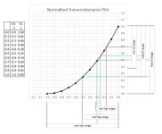
Looking at the second page of the datasheet https://pdf.datasheetcatalog.com/datasheets/nec/2SK68A.pdf you see this curve:

showing that all ranks have essentially the same transconductance at the same current. That's by far the most important parameter for amplifier use.
The source will settle about 0.4 V higher than with L rank devices, but due to the large voltage across the tail resistor, that will only increase the tail current by 3 % or so. Chances are the circuit can handle that with no problems.
Looking at the second page of the datasheet https://pdf.datasheetcatalog.com/datasheets/nec/2SK68A.pdf you see this curve:
showing that all ranks have essentially the same transconductance at the same current. That's by far the most important parameter for amplifier use.
The source will settle about 0.4 V higher than with L rank devices, but due to the large voltage across the tail resistor, that will only increase the tail current by 3 % or so. Chances are the circuit can handle that with no problems.
But now the jfets operate in a less linear (closer to Vpo) portion of the transconductance characteristic, adding more distortion. Same for #3. It's always a trade off.The source will settle about 0.4 V higher than with L rank devices, but due to the large voltage across the tail resistor, that will only increase the tail current by 3 % or so. Chances are the circuit can handle that with no problems.
The OP tries to have the replacement (higher grade) in the same section of the transconductance curve.
Looking in the vicinity of 0.75 mA drain current, the curves look similarly curved to me, they just shift to the left. Besides, the input stage of a RIAA amplifier with overall feedback isn't likely to distort much.

The outward view looks similar, but it's not the 'curvature', but the actual setpoint on that very curve. Peter van Willenswaard (you sort that out) claimed the steeper up that hill the better the performance (more linear transconductance, up to 0.7Idss^), and for many good reasons: the higher the Id-set, the less distortions - how far do you dare to go?Looking in the vicinity of 0.75 mA drain current, the curves look similarly curved to me, they just shift to the left. Besides, the input stage of a RIAA amplifier with overall feedback isn't likely to distort much.
Oh yes, the overall white washining feedback will cover it all. Certainly if the first stage loose 33% gain. I don't buy this yfs reasoning, that's only overal (closed loop) performance. It should be rock solid open loop first, and then the closed loop specs. 'Looks' similar is... cough... sorry folks
If I understand it correctly, the thread starter is trying to repair an amplifier with the parts he/she/they/it can get, not to redesign one. If you want to stay as close as possible to the original design, just bias the JFETs to a point where the transconductance and curvature is about the same as in the original design.
The replacement JFETs behave essentially the same as the originals, but with a 400 mV or so gate-source voltage shift. Compensate out that 400 mV by replacing both JFETs and you should have an amplifier that performs very similarly to the original.
If you want to redesign it instead of repair it, then you end up at a different solution.
the vds is hardly defined by pinch off voltage as we have a large resistor in the tail coming from a -29V rail. so the only concern is to keep the same yfs (transconductance) at the calculated current. 29V/ 13.3k or about 1.1mA per device. nothing critical here
Thank you for this; Since I am not very knowledgeable in this area, I just want to clarify that you are saying with the new N rank devices, if I increase the drain current via drain and source resistor adjustments to 1.1 mA from 0.75 mA, the JFET's will be operating in the same region as the original devices?
If I understand it correctly, the thread starter is trying to repair an amplifier with the parts he/she/they/it can get, not to redesign one. If you want to stay as close as possible to the original design, just bias the JFETs to a point where the transconductance and curvature is about the same as in the original design.
The replacement JFETs behave essentially the same as the originals, but with a 400 mV or so gate-source voltage shift. Compensate out that 400 mV by replacing both JFETs and you should have an amplifier that performs very similarly to the original.
If you want to redesign it instead of repair it, then you end up at a different solution.
Thank you so much for your help; I have learned a lot from what you shared and I appreciate your simple approach. Your analysis of the curves in the datasheet make sense to me. It sounds like you are saying that with the new devices and stock values, the performance will be "close enough" to stock. What happens if I want to at least meet the stock specifications? It sounds like increasing the current a bit and adjusting the drain and source resistor values could be beneficial.
What I meant is that with just both JFETs replaced, the difference with the original will be very small indeed. If you measured the performance parameters, they would probably all fall somewhere in the distribution of the same parameters of unmodified units.
If you want to improve the performance compared to the original, there are many things you could change. Using N rank JFETs and biasing them at a higher current will reduce their distortion and noise somewhat compared to the original design, but I doubt that they dominate the distortion anyway and I'm quite sure they don't dominate the noise when there is a real MM cartridge connected to the input. Thermal noise of the cartridge and 47 kohm resistor dominate when there is no record playing, record surface noise dominates when it is playing.
If you want to improve the performance compared to the original, there are many things you could change. Using N rank JFETs and biasing them at a higher current will reduce their distortion and noise somewhat compared to the original design, but I doubt that they dominate the distortion anyway and I'm quite sure they don't dominate the noise when there is a real MM cartridge connected to the input. Thermal noise of the cartridge and 47 kohm resistor dominate when there is no record playing, record surface noise dominates when it is playing.
Thank you Marcel. That makes sense; I like this solution and I'm hoping my sensitive ears don't notice a different. Now, suppose I did want to try and increase the current to maintain the stock transconductance as the member bassreflex suggested. At about 1.1 mA per device, can I just do so by lowering the value of the 22K drain resistors or would I also need to change the source / tail resistor? What I don't understand is if the source voltage will self bias to an ideal value even though the current is increasing through the source tail resistor tor if the source resistor needs to be carefully calculated to hit the target source voltage of 0.3 -0.4 volts
Last edited:
The outward view looks similar, but it's not the 'curvature', but the actual setpoint on that very curve. Peter van Willenswaard (you sort that out) claimed the steeper up that hill the better the performance (more linear transconductance, up to 0.7Idss^), and for many good reasons: the higher the Id-set, the less distortions - how far do you dare to go?
Oh yes, the overall white washining feedback will cover it all. Certainly if the first stage loose 33% gain. I don't buy this yfs reasoning, that's only overal (closed loop) performance. It should be rock solid open loop first, and then the closed loop specs. 'Looks' similar is... cough... sorry folks
Thank you, this makes sense as well but at what point is the current too much or there is no benefit beyond? Elliot Sound recommends around 50% of the IDSS spec. I think we can see the operating point original design did not occupy the steep part of the curve. Why would Kenwood lose out on specs they could market on a flagship piece?
Thank you for all of this, but in the end, this is a little beyond what I would like to do. I would like to keep it close to stock with only basic adjustments at most.2SK68A (L): Vpo = -0.45, Idss = 2.2mA... what do you specify with the "ON: 0.22V"?
unknown jF: Vpo = -0.80, Idss = 5.5mA... what do you specify with the "ON: -0.1V"?
Why?
Calculations are ok.
You have to maintain that Vds indeed.
Why 50% of Vpo? That will be 0.4V instead of the original 0.13V -- no problems for the source resistors, a marginal difference.
But this increased drain current is 330% more then the original, from 0.75mA to 2.5mA -- that's a challenge.
And here you are loosing some (22k/6.6k=) 3.3x open loop gain.
Keep in mind that this a RIAA pre-amp -- it's riaa-correction needs 40dB, raising the signal from 2.5mV to 150mV another extra 16dB at least!
In general, overall open loop gain should be well above 60dB. By reducing the open loop gain, you can expect increased distortion and, not really a bonus, added noise due to this considerable gain reduction in the very first stage!
To exactly calculate the voltage at the Ri-109/-111/-113 junction:
Vj = { (R111 * R113) * Vs + (R109 * R111) * Vn } / { (R109 * R111) + (R111 * R113) + (R109 * R113) }
Vs: Vsources (+0.13Vdc); Vn: negative rail (-29Vdc)
So, in the original situation Vx = -14.27V
Changing R109 from 10k to 1k58 yields a Vx = -7.579V (close enough!).
However, the long tail pair can 'clearly see' a resistor and not a current source. This will effect the overall operation of this first stage (to an unknown result).
Conclusion:
If you replace the 2SK68's, exchange the Ri-109/-111/-113 parts for a fixed/adjustable two/three-pin current source (readily available) and use one too in combination with a pnp current mirror to 'subtract' the surplus current (2.5 - 0.75 = 1.75mA) from the drians to maintain the 22k resistors.
They will add a very little noise (the CM), but the RIAA amp itself will remain the same.
Analysis shows (Normalized Transconductance Plot) that that is not necessarily the hotspot for all situations: the higher the setpoint, the more linear the curve.Elliot Sound recommends around 50% of the IDSS spec.
A matter of taste? I prefer the setpoint at 1/4 Vpo, which results in sufficient dynamic input range and the upper (more linear) 70% of the output range.
It has to do with the non-necessary-to-be-selected parts as 'pre-selection' is expensive.I think we can see the operating point original design did not occupy the steep part of the curve. Why would Kenwood lose out on specs they could market on a flagship piece?
It is a commercial enterprise, it's goal is to make profit.
Attachments
Thank you, that makes sense. So perhaps I want to increase my gate - source differential. How do I go about properly determining this. Will the JFET naturally self bias there or do I need to set the drain and source resistor exactly to hit the target source voltage?
In #2 I've discussed most issues to take care of.
The main restriction in this circuit combined with another type of Jfet are the 22k drainresistors. With such a high value, a very low draincurrent is required. You already hit that in #13. In general (from a manufacturers viewpoint), the lower the setpoint, the universal the circuit - no pre-selection needed.
With the 22k drainresistors, using Jfets with a (relative) high (or higher then the original) Idss requires them in a more curved (lower) section of the transconductance plot, causing more open loop distortion. This will happen with an unchanged LTP current source value.
Lowering those drainresistors to your proposed 6k6 allows Jfets with a higher Idss, but you will loose open loop gain, causing more closed loop distortion (and more noise). The LTP current source must be adjusted to this new value.
The best option is to find parts with almost the same specs, both Idss and Vpo. If that's not possible, you have to except either increase of distortion or find a workaround - the employment of current sources in parallel with the drainresistors to cope with the higher draincurrent ('current-suckers'... sorry mods) is an option here.
If you accept the lower open loop gain with the 6k6 drainresistors (the easy way, take 6k8 or 5k6), the best route is to measure the exact specs of the new Jfets to calculate the best LTP current and the involved resistors. It will be obvious that the actual sourcevoltages will differ (with a higher Idss comes often a higher Vpo), but that will settle itself (only during powering on & off the closed loop cannot keep the gates equal, so there's always some 'designrisk - that's the reason you may find sometimes two antiparallel diodes between the gates of the differential)'.
It is important however to keep the value of R109 as high as possible, R111 & R113 together with C103 act as a filter.
If R109 is maintained at 10k, R111 and R113 will be substantially lower in value, forcing C103 to a higher value to maintain the Fo of the filter.
Everything is 'glued' to eachother. And this is only the first stage...
What type of Jfets are you intending to use, and (if already on your desk), what are their Idss and Vpo values?
(If you have a bunch of them, the ones with the lowest specs may have the highest gm!)
The best option is to find parts with almost the same specs, both Idss and Vpo. If that's not possible, you have to except either increase of distortion or find a workaround - the employment of current sources in parallel with the drainresistors to cope with the higher draincurrent ('current-suckers'... sorry mods) is an option here.
The same as what? As each other?
As the original parts & each other, as they are in a differential.
That's a bit to obvious to discuss.
That's a bit to obvious to discuss.
The new JEFT's are 2sk68a N Rank. I gave the measured specs in my original post. I think I might learn more efficiently if you were to recommend the resistor values for the new devices. Then I could reverse reason through the choices. From what I can tell, we only need to marginally raise the current to maintain the original distortion performance at slightly less open loop gain. We could target 1.1 mA drain current through 15K drain resistors. Then, what does R109 need to be and how do we reason through this optimization? Is it simply calculating its values at the given current (2.2 mA) to give a target source voltage (let's say 1/4 pinch off voltage). Since Vgs Off is 0.8 volt, then would we simply target a gate voltage of 0.6V?
- Home
- Design & Build
- Electronic Design
- Seeking help with reconfiguring jFET differential input for new jFET Parameters