When calculating the load, don't forget to take into account the following stage. For example, your 12au7s don't see a 38k load, they see 38k||100k. Still an OK load for this tube, but in other situations it could cause things to behave much different than you expect.
You coudl also remove the 47u cathode cap from the 12AU7, to encourage a modicum of self-balanicing.
Hi again
I posted a few days ago to say hello and describe my project, a KT88 PP ultralinear amp, which also happens to be my first valve amp build.
Nothing like jumping into the deep end.
Since then I've been reading a lot to achieve a sufficient understanding of preamp circuits. I could easily have just picked a schematic off the internet and built that, but I wouldn't have learned anything by just assembling a jigsaw puzzle. So I've been doing a lot of reading, a lot of modelling in TubeCad, and checking over my calculations.
Finally I have a preamp circuit that I am reasonably happy with on paper. The topology is simple: 12AX7 initial gain stage using the grounded cathode topology, followed by a balanced load inverter using the other half of the 12AX7, followed by a 12AU7 grounded-cathode driver stage.
It's all described in my blog post on the subject - what I'd really appreciate is for someone in this helpful community to look over my shoulder and let me know whether this looks OK or whether I've made any mistakes that'll bite when I come to build it.
So thanks in advance for anyone who takes the time 😀
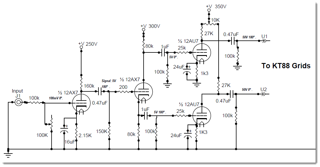
Suggested preamp stage
The volume control is more appropriate to o'scope vertical amps, though usually buffered, and using smaller resistors for less noise. You don't need much range with o'scopes: just enough to keep the trace on the screen. You'd do better with the alternative I used here (attached). In this case, the pot is a 100K linear taper pot with the wiper paralleled with a 16.8K metal film resistor to give a log taper characteristic. You can include a small (47R) resistor to prevent bottoming out. It's also useful in that you automatically have a guard resistor that can prevent the control grid from floating should the wiper lose contact with the track.
I really don't like using 12AX7s as cathodynes or cathode followers. It would be better to use a trioded 6AU6 as a cathodyne, and replace the up front 12AX7 with a 6AV6 (be sure to connect the diode plates to the cathode). If you don't want another hole in the chassis, then use a 12DW7. This is a dual that includes a section like the 12AX7 and 12AU7 that was designed specifically for use as a gain stage driving a cathodyne.
Capacitor coupling the cathodyne like that doesn't work unless you float the grid positive, otherwise there is not enough headroom, and 80K in the tail with the grid at DC ground puts the 12AX7 almost into plate current cutoff. It would be better still to DC couple here. That gets rid of one RC phase shift network that will compromise low frequency stability under gNFB.
I would get rid of the 12AU7s. It is difficult to get good audio performance from what is essentially as RF/quasi-digital type. Schemos where 12AU7s are used are mostly RF designs (oscillator/buffers, Class C drivers/frequency multipliers, singly balanced mixers/demodulators, nonsinusoidal oscillators/squaring circuits, one shots, flip-flops and RS latches). Most audio applications are either cheap consumer grade equipment or guitar amps. The 6FQ7 would be a better choice as a medium level gain stage here. It would also be better to use the 6FQ7 as a differential gain stage. That way, you wouldn't need any sort of balance adjustment.
Attachments
"Valve Amplifiers" by Morgan Jones (4th edition) [] is a book you should own and study carefully.
Thanks for the steer in that direction. Bought that and also the companion "Building Valve Amplifiers" from the same author.
I also find that Merlin Blencowe's Designing High Fidelty Tube Preamps is very helpful. Merlin Blencowe's explanations are easier for me to follow than Morgan Jones', but that's just me. Having the two takes on explaining similar material has helped me quite a bit. I've found it's well worth having both.
--
--
I also find that Merlin Blencowe's Designing High Fidelty Tube Preamps is very helpful.
Agree totally, I also would want to have both, but Merlin's excellent book is probably more useful for preamp design than power amp front ends.
The other must-have IMHO is Crowhurst's "Understanding Hifi Circuits."
Completed schematic
Following the helpful advice from several members on this forum, I've re-worked my schematic and completed it into a form that I believe is ready to build.
Quite a few changes after doing a lot of reading:
This is the schematic. Completely cooked up from scratch. Much work with calculators.
Bias points are 0.6mA for the 12AX7 and 5mA for the 12AU7
Any gotchas here I missed before I get soldering?

Following the helpful advice from several members on this forum, I've re-worked my schematic and completed it into a form that I believe is ready to build.
Quite a few changes after doing a lot of reading:
- Changed Circuit diagramming software to Tinycad (and made up my own parts library for the transformers)
- Added KT88 final stage
- Re-arranged 12AU7 driver stage layout in the diagram
- Changed all resistors to preferred values, recalculated bias and voltages as required
- Added theoretical voltage reference points through the circuit
- Calculated power dissipation across all resistors
- Calculated DC voltage across all capacitors
- Added voltage dividers to power the gain, splitter and driver stages (modeled in PSUD2)
- Added power supply and KT88 bias adjustments
- Added NFB
This is the schematic. Completely cooked up from scratch. Much work with calculators.
Bias points are 0.6mA for the 12AX7 and 5mA for the 12AU7
Any gotchas here I missed before I get soldering?
Why the 47uF bypass cap on the tail impedance of the LTP driver stage? Also, 1.2K is a pitifully small tail impedance. A neg. power supply would allow for a larger resistor or better yet a CCS (constant current sink). You should read up on differential "long tailed pairs" and how to optimize.
Why the 47uF bypass cap on the tail impedance of the LTP driver stage? Also, 1.2K is a pitifully small tail impedance. A neg. power supply would allow for a larger resistor or better yet a CCS (constant current sink). You should read up on differential "long tailed pairs" and how to optimize.
'tis not actually a LTP... I could be slightly misleading in the way I've drawn the circuit. The grid of the second 12AU7 is driven the same way as the first... this is just one grounded cathode per phase
Unless I'm missing something?? Which is entirely possible
What is the purpose of R20, R23, R25?
Why using the odd bias method for the split load inverter? Why not use, either a grid leak connected to a cathode resistor in series with the 82k resistor, (as is the normal way and described by e.g. Philips in tube data books) or direct coupling from the preceding stage as in the Williamson?
For the driver please study the Williamson amplifier which uses a balanced driver with a common cathode resistor without decoupling, there are reason to do it like that, one advantage is that you can get some reduction of 3rd order distortion. see here https://ideas.home.xs4all.nl/amps/pages/chapt3.html
What is the purpose of R20, R23, R25?
These 100K resistors - while admittedly wasting a bit of power - are there as the principal load seen by the voltage divider, they will draw around 3x more current than the valve will and thereby reduce the valve's influence ocer the voltage. These may not be needed owing to the presence of the capacitors (C10, 11, 12). I've seen some circuits with these resistors in them, but as you have observed, they may not be necessary.
Why using the odd bias method for the split load inverter? Why not use, either a grid leak connected to a cathode resistor in series with the 82k resistor, (as is the normal way and described by e.g. Philips in tube data books) or direct coupling from the preceding stage as in the Williamson?
I've seen the direct coupling approach, but in my case the anode of V1a will be at about +160V and the grid of V1b needs to be at around +45V, so I can't see how direct coupling would work here. As for the Grid leak / cathode resistor approach, I'll follow that up - thanks for the idea.
For the driver please study the Williamson amplifier which uses a balanced driver with a common cathode resistor without decoupling, there are reason to do it like that, one advantage is that you can get some reduction of 3rd order distortion. see here https://ideas.home.xs4all.nl/amps/pages/chapt3.html
I have this same message some others as well - I've removed this cap already in my schematic and it won't be included in the circuit. I'd intended to remove it prior to posting up this revision but overlooked it.
I have never seen these resistors at the anode, (like your R20 etc) in any tube design, probably your intended purpose is to get a stable anode voltage but it is not really necessary as the gain of the tube is affected very little by minute variations in anode voltage. Do you have a link to any design where it is used? I am interested as I have never seen it.
I have never seen these resistors at the anode, (like your R20 etc) in any tube design, probably your intended purpose is to get a stable anode voltage but it is not really necessary as the gain of the tube is affected very little by minute variations in anode voltage. Do you have a link to any design where it is used? I am interested as I have never seen it.
The quiescent current of V1a is 0.6mA. At 250V according to Ohms law this represents a resistance of 416.7K, comprised of the Anode resistor, the valve itself, and cathode resistor.
Without the 100K load resistor, a voltage divider network to get 250V from the 500V B+ supply would need a 420K or 500K resistor. This would severely limit the current available to charge C10
Two scenarios modelled in PSUD2.
Without the 100K load resistor, even if I drop the capacitor to 16µF, the charge time until we have +250V is around 20sec

With the 100K load resistor, I can increase the capacitor to 33µF and still get a much faster charge time:

This is my reasoning anyway - but am well prepared to be told I've overlooked something...
Last edited:
I would use the 1/2 12AU7 for more gain after the 12AX7 and then feed the other half 12AU7 used as splitter concertina with about 6 ma bias on it.
As it sits, the gain between both halves is not guaranteed to be the same.
it also requires 1 less triode.
As it sits, the gain between both halves is not guaranteed to be the same.
it also requires 1 less triode.
Here is what I would build, shown with 4ma bias @300v
I pasted from another cct , 90 v on 12AX& should be 200v *6C33 error sorry
I pasted from another cct , 90 v on 12AX& should be 200v *6C33 error sorry
Attachments
Last edited:
NFB will be zero unless you have some unbypassed resistance in V1a cathode.
There's a total of four high-pass filters in this circuit if we include the OPT, so low-frequency stability with feedback will be very difficult to achieve. If I was doing this, as a minimum, I would rejigger the biasing so I could direct-couple V1a to V1b. Better yet, why not make both V1 and V2 into good diff-amps with direct coupling between them? Your -80V source is good for a transistor CCS at V1 tail, and the V2 tail could be a resistor for simplicity. Feedback could go to the opposite grid of V1.
I know I'm messing with your line of thought, but you could be a great deal more confident of building a satisfying amp this way. There are many other ways, of course. This is just an approach suggested by the components you've already selected.
NFB will be zero unless you have some unbypassed resistance in V1a cathode.
Noted
If I was doing this, as a minimum, I would rejigger the biasing so I could direct-couple V1a to V1b.
Yeah been playing with that idea - a long calculator-and-TubeCad session. I can take the B+ on the first stage from 250 to 200v easily enough, keeping the anode resistor at 150K this gives a plate voltage of +125V. This means if I am to DC-couple, I need a cathode voltage on the next stage of around 128V
This I haven't been able to manage without resorting to a B+ of 400V on that stage combined with stupid load resistors (Ra and Rk of around 130K)
I can't help feeling like there's some crucial concept I am missing here...
Tubelab (George) participated in a thread where he helped member Chrish design a push-pull 6L6GC class AB2 amp with a 6SN7 LTP feeding a 6SN7 differential pair driver. Read into the thread to get to Chrish's final version. I'm sorry I don't remember exactly where it is in the long thread.
http://www.diyaudio.com/forums/tubes-valves/133034-6l6gc-ab2-amp.html
--
http://www.diyaudio.com/forums/tubes-valves/133034-6l6gc-ab2-amp.html
--
Yes but what is the problem with that?The quiescent current of V1a is 0.6mA. At 250V according to Ohms law this represents a resistance of 416.7K, comprised of the Anode resistor, the valve itself, and cathode resistor.
Without the 100K load resistor, a voltage divider network to get 250V from the 500V B+ supply would need a 420K or 500K resistor. This would severely limit the current available to charge C10
What is the problem? heating time of the tubes is longer than thatWithout the 100K load resistor, even if I drop the capacitor to 16µF, the charge time until we have +250V is around 20sec
With the 100K load resistor, I can increase the capacitor to 33µF and still get a much faster charge time:
I would probably use as high as possible anode voltage on the first tube as it minimize distortion. about 400V would allow 50V drop over the resistor before the capacitor then use at least the same or preferably more for the inverter and the driver. High available voltage for the inverter allows for easier direct coupling from the preceding stage. BTW I agree with Stocktrader200 that 12AU7 would be better as inverter, I used the same setup as he suggest in my original OTL 6C33C OTL although there I used a SRPP coupled 12AX7 as input, I have also used it as differential stage allowing for balanced input.
If you want low distortion from a 12AX7 then you need a high anode resistance, which means either a high supply voltage or a CCS. You have deliberately designed for a low supply voltage to this stage, and then had to use a low value anode resistor. Why set out to reduce the performance of the stage?
You have made the same mistake with the second stage.
Anyway, you will struggle to achieve stability with this circuit. Four stages plus an OPT means far too much phase shift at frequency extremes. That is why almost all valve amps use three stages.
You have made the same mistake with the second stage.
Anyway, you will struggle to achieve stability with this circuit. Four stages plus an OPT means far too much phase shift at frequency extremes. That is why almost all valve amps use three stages.
- Status
- Not open for further replies.
- Home
- Amplifiers
- Tubes / Valves
- Seeking a peer review for my preamp design