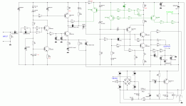
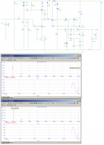
Just a result of some my experiments.. Transistors only (and not so many of them). Also I'm not very sure if it clean SE, but its output stage is not usual push-pull, more exactly SE with local current servo loop that prevents transistors cut-off even if output current exceeds quiescent current (something like Super-A).
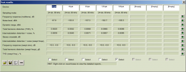
Specs (measured with 7.2Ohm load):
Quiescent DC current: 450mA
Input power: 35VAC, uses virtual ground so requires fully separate transformer windings for different channels.
Max output Vpk measured before clipping: >18V
Schematics and measurement results attached. Green parts on principal - overcurrent protection (can be simple removed). Also sprint layout 6 file attached.
Note that given schematics optimized basing on experiments, simulation with microcap provided rather different optimal values for current mode and correction. And yes, I understand that using BSS92 at preout stage looks rather strange, but it produces best results while still operating in SOA (I used BSS92 produced by Infineon, all 2sc/2sa transistors - Toshiba's).
Attachments
-
 SeeA_principal_1.1.GIF51.3 KB · Views: 380
 -
 photo.jpg56 KB · Views: 186
 -
 meandr_5Vpk.png3.3 KB · Views: 117
 -
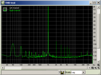
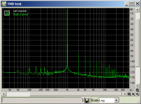 rmaa_THD_18Vpk.png31.9 KB · Views: 88
 -
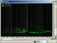 rmaa_THD_12Vpk.png17.7 KB · Views: 96
 -
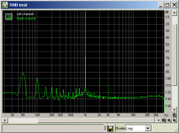
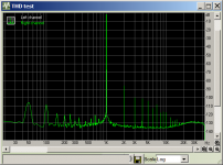 rmaa_THD_8Vpk.png17.5 KB · Views: 299
 -
 rmaa_THD_4Vpk.png17.5 KB · Views: 305
 -
 rmaa_THD_2Vpk.png17.4 KB · Views: 314
 -
 rmaa_overall.png55.6 KB · Views: 359
 -
super_a_feb7_1.lay6.zip78 KB · Views: 57
Last edited:
Pretty cool 😎
Did you try to measure THD at 20KHz?
It would be also interesting to see a 20KHz square wave response.
Did you try to measure THD at 20KHz?
It would be also interesting to see a 20KHz square wave response.
Schematics and measurement results attached. Green parts on principal - overcurrent protection (can be simple removed).
Can you please arrange the direction of electrolytic caps in a way so that they will not burst on power up? Just a suggestion ..
I've always draw filled part as positive usually its rather obvious, but you're right, better to follow standards.. but ...Can you please arrange the direction of electrolytic caps in a way so that they will not burst on power up? Just a suggestion ..
...and time is out.The administrator has specified that you can only edit messages for 30 minutes after you have posted.
BTW in layout file holes labeled correctly and unambiguously with '+' signs🙂
About 20KHz square - currently I don't have such generator, but will try to make one on logic chips.
Do you want to discuss the topology?
PS you can edit the first post of your own thread any time (not sure about the pictures).
PS you can edit the first post of your own thread any time (not sure about the pictures).
That message I'm getting exactly when pressed 'Manage attachments' button in 'advanced' edittor (non-advanced doesn't have attachments editing possibilities).
Regarding discussing - that is main purpose of web forums, isn't it?
But the main points of given topology was simplicity, minimal elements in nfb loop and stability with capacitive load (even if remove output filters). Its not hard to achieve more linearity if decline any of goals above.
Regarding discussing - that is main purpose of web forums, isn't it?
But the main points of given topology was simplicity, minimal elements in nfb loop and stability with capacitive load (even if remove output filters). Its not hard to achieve more linearity if decline any of goals above.
Regarding discussing - that is main purpose of web forums, isn't it?
But the main points of given topology was simplicity...
Some people just want to show their new developments.
Not everybody is prepared for thorough questions.
If you address simplicity: the input stage, emitter follower T1 and its current source T2
isn't simple at all and even has two coupling caps. It is outside the feedback loop.
Why do you use it? Is it required for high input impedance?
More questions may follow.
About T1/T2. There're also more important elements after them - RC filter R9/C6-7.
On one side it filters out high-frequency noise that can arrive from input. NFB loops are very sensitive to HF noise - even when their spectrum lays outside of hearable region intermodulations caused by them may appear in lower range. And intermodulation level caused by HF signal much larger than on sonic band.
Also there is other side. I wanted to make NFB loop faster and decouple it from output of emitter follower on high frequencies, and C6/C7 makes T4 to work better in common base mode for high-frequency NFB signal coming to its emitter.
So this unusual input stage makes NFB loop faster and more stable, while on the other side limiting whole amplifier signal bandwidth (but this limiting is far enough off hearable range).
Also I'm considering using PNP for input follower - this should decrease a bit total HD due to opposite phases of HD products introduced by pre- and power- stages in such case..
Last edited:
OK, it is often desirable to have some input filtering.
Do you agree that it is possible to use T1, T2 and T4 as an ordinary differential amp with
emitter current source having essentially the same properties as far as signal path is
concerned but with reduced complexity at T1 input probably (but input filter still retained)?
Did you compare the differential pair to your separation solution?
Looking at the diagram in total I can not see how a dc zero is established at the output.
A zero adjustment is also not visible and no means to prevent any drift of the output dc.
Looking at the diagram in total I can not see how a dc zero is established at the output.
A zero adjustment is also not visible and no means to prevent any drift of the output dc.
T4,T5,T9 establish a feedback loop the same as any singleton input style amp.
T4,T5,T9 establish a feedback loop the same as any singleton input style amp.
But where is the reference to zero?
The base of T4 is set to a voltage that is Vbe + the voltage drop of R14 above 0V. This is usually done with an adjustable voltage divider, see original JLH amp. Here it is done with the divider at the base of T1 which will add another Vbe to the reference voltage.
Have a look at the negative speaker terminal. It is a capacitor coupled output. The output voltage works out to around 22 volts which is close to 1/2 B+.
Sure its possible to use output stage with differential cascade but.. here its used in such way🙂 cuz if using diffcascade in usual small-current mode - it will not be able to drive T5's input capacitance fast enough directly, thats actually a reason why 40mA used as a quiescent current for T3-T4 now. And having diffcascade with such working current would again require something to have high-enough input impedance.Do you agree that it is possible to use T1, T2 and T4 as an ordinary differential amp with
And yes, this amp has a DC coupled ground so no need to worry about zero-reference, except it affects clipping symmetry
In real-life its 23.8V likely because my mpsa06's hfe appeared larger than in simulator's modelHave a look at the negative speaker terminal. It is a capacitor coupled output. The output voltage works out to around 22 volts which is close to 1/2 B+.
Last edited:
Agree, if the supply is floating and speaker is capacitor coupled, DC offset is not a problem (thought this was not sure from the diagram).Have a look at the negative speaker terminal. It is a capacitor coupled output. The output voltage works out to around 22 volts which is close to 1/2 B+.
DC balance still is undefined, this means that dynamic range and clipping behaviour may be impaired and it is supply dependent.
40 mA - not too shabby for an input stage ..40mA used as a quiescent current for T3-T4
You mean AC coupled output?And yes, this amp has a DC coupled ground so no need to worry about zero-reference, except it affects clipping symmetry
This current actually works not only for input stage, but for output too since its all drained into T10.40 mA - not too shabby for an input stage ..
However its possible to turn output stage into highly linear follower by removing R11/C9, reducing R14 to ~20ohm, changing C10 to some bigger value and adjusting R3/R4 to keep ground somewhere in the middle of +/- (see attached pic). Also input follower in this case should be replaced with something else cuz it will be too non-linear with large level large signals. But I didn't try this yet. Also simulation shows that stability with capacitive load in this case will be in some degree worse in follower mode, as expected, so output filer inductance likely should be increased to keep it stable with usual load. The another good thing with follower mode that all that 40mA of input stage current will directly help output transistors to drive the load.
yesYou mean AC coupled output?
Attachments
- Status
- Not open for further replies.
- Home
- Amplifiers
- Solid State
- SeeA amplifier (Single end/energy-effective A)