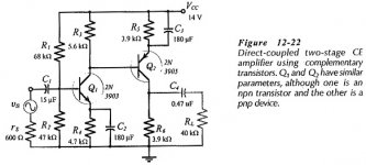
Like the subject says I'm looking for a good tutorial on how to design something simple like this Two Stage Direct Coupled BJT Amplifier Circuit
For example how do you arrive at the bias voltage for Q1? The divider sets the bias voltage but what parameter in the datasheet would give you a clue? Thanks.
For example how do you arrive at the bias voltage for Q1? The divider sets the bias voltage but what parameter in the datasheet would give you a clue? Thanks.
You want the first stage collector's DC voltage to be around half of the supply voltage,
for maximum AC voltage swing there. The DC base bias voltage for the second stage
is the DC collector voltage of the first stage, since they are directly coupled.
This should help for the first stage only.
Two-stage CE amplifier
for maximum AC voltage swing there. The DC base bias voltage for the second stage
is the DC collector voltage of the first stage, since they are directly coupled.
This should help for the first stage only.
Two-stage CE amplifier
Last edited:
Not really. The second stage is the output, and that needs to have the collector set to half way between the emitter voltage and the collector maximum voltage. As Q2 is a PNP the emitter is near Vcc+ and the collector connects to ground through a load resistor.
The first stage feeds the second at whatever base voltage is chosen.
To set the bias voltage on Q1 you need the base-emitter on-state voltage. Many take 0.6V as a guide or starting point. Then you need to choose what emitter voltage to run at. If that were zero then changes in Vbe would swing the collector current up and down with temperature. So as a rule the emitter needs to be more than the base voltage - say 1V- so that changes with temperature don't change the current much.
Then the emitter resistor is chosen according to the current wanted.
A typical 2 stage amp might use 200uA in the Q1 and 2mA in Q2 so that the lower current has lower noise and the higher current provides for a suitable output swing, but these can be varied.
That makes the starting point of the design something along the lines of
Q1 emitter voltage 1V, current 200uA therefore R=4.7k (nearest preferred value).
Base voltage =emitter+0.6 =1.6V
Since the base current is much smaller than the emitter current the bias resistors need only conduct 1/10 to 1/20 of the emitter current, depending on the transistor gain (hFE).
If you used a high gain low noise transistor for Q1 like the BC549 the bias current could be 10uA so the lower base resistor is 1.6/.01=160k. That allows you to calculate the upper bias resistor.
Similarly, if Q2 works at 1V below the rail voltage its base will be 1.6V below, so you can go through the same thought procedure to work out the remining values. The collector resistor of Q2 needs to set the collector voltage to the mid point of the output swing. If the supply voltage were 12V the emitter of Q2 is 11V and the base 10.4V and the collector load resistor would be 11/2V divided by the 2mA current.
....something simple like this Two Stage Direct Coupled BJT Amplifier Circuit
There are three plans on that page (which?), and they are all pretty bad. Work out its/their operating point for mental exercise and then move on.