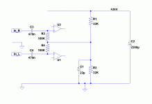
They set a difference of DC potential between the outputs, so that the current source/sink has sufficient room to operate.Elvee, pardon my ignorance, but what is the purpose of R8/9?
The lower the potential, the more efficient is the circuit compared to a standard SE amplifier, but the less tolerant it is to non-correlated L-R signals.
Thanks Elvee, its devilishly simple! I like it a lot 🙂 Especially the use of parts intended for radically different purposes 😉
Tony.
Tony.
Could this be used to drive a 2 ohm load? If so how many watts would you be able to get out of this amp?
This seems like a novel and affordable way to build an amp. I think that after the design is optimized you should make a few boards for everyone.
This seems like a novel and affordable way to build an amp. I think that after the design is optimized you should make a few boards for everyone.
The maximum output is limited by the peak output current that the amp can deliver.
Pmax = Ipk^2 * Rload / 2.
1.5Apk results in a maximum of 1.5W into a 2r0 load.
4r0 allows 3W of maximum output
8r0 allows 6W of maximum output.
If the output current can be doubled, then the maximum output power is quadrupled.
Pmax = Ipk^2 * Rload / 2.
1.5Apk results in a maximum of 1.5W into a 2r0 load.
4r0 allows 3W of maximum output
8r0 allows 6W of maximum output.
If the output current can be doubled, then the maximum output power is quadrupled.
This variant is a single-ended one, and the effective peak current is only ~800mA.
This yields 2.5W into 8R.
The complementary variant is a push-pull, and delivers more power
This yields 2.5W into 8R.
The complementary variant is a push-pull, and delivers more power
I found it rather strange that this hasn't really caught on, looks like the best thing since CMOY or Gainclones to me!
Other than that LM317s needs a bit a attention in regards to isolation when mounting to heatsinks (output is tied to tab), this thing looks easy enough to wire point to point and risk for failure seems low.
I'll definitely build one and hopefully bring some attention from the headphone board.
Other than that LM317s needs a bit a attention in regards to isolation when mounting to heatsinks (output is tied to tab), this thing looks easy enough to wire point to point and risk for failure seems low.
I'll definitely build one and hopefully bring some attention from the headphone board.
I recommend the following steps if you want to use this amplifier with a single 24V supply.Pardon my language.
When I first looked at the SE class A I was under impression that since 2 channels are have different potentials, each had to be referenced to different rails if single supply was used.
But it just occurred to me that this made no sense at all! I'd be able to flip polarity on the lower output cap and reference both channels to V-, is that right?
Since I am coming from a single supply (have to many laptop PSU lying around), I'd be using either a TLE2426 rail splitter for input ground or a equal value resistive splitter, but would it make more sense if some uneven resistor divider was used to set the opamps' output differently in the first place?
I am not familiar with introducing DC to the inverting input, but it looks like 390k+10k || 100k divider would provide 4.8V from the rails. This looking rather close to the rails so I may be wrong.
Note that SMPS's have the unfortunate tendency to inject nasties through their "Y" capacitors, and the result could be disappointing.
The V- rail will now become the reference potential.
-Connect to V- the cold side of the loads, and flip the polarity of C2
-Connect C3 and C4 to V-, flip the polarity of C3
-Use a bias network on the input as outlined on the schematic, and refer the inputs to V-
These modifications should be "transparent" provided you use a good local decoupling of the supply (2200µF)
Attachments
I found it rather strange that this hasn't really caught on, looks like the best thing since CMOY or Gainclones to me!
Other than that LM317s needs a bit a attention in regards to isolation when mounting to heatsinks (output is tied to tab), this thing looks easy enough to wire point to point and risk for failure seems low.
I'll definitely build one and hopefully bring some attention from the headphone board.
agreed!
I think this may be the new hot thing to compete with chipamps.
just to share and spur more interest.
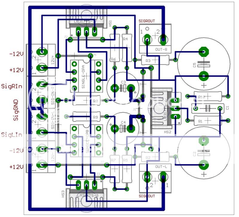
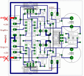
single side layout using 2 single op amp coming from a non EE trained personnel.
single side layout using 2 single op amp coming from a non EE trained personnel.
Looks nice and compact.
One or two remarks:
-I don't see a continuity between the power supplies and signal grounds.
-If the power supplies are off board, which is the case here, it is a good idea to provide a local decoupling, 2x100µF (or more) for example.
-The inputs are DC- coupled. This may be fine in many cases, but it could be problematic too.
Including an AC coupling on board would be a good idea, it can always be strapped if not needed.
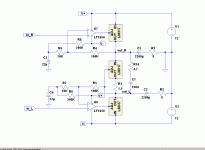
-Remember that in this version, for 8R speaker driving, the total quiescent power dissipated is ~20W, which requires hefty heatsinks (and ~1A supplies).
For 32R loads, R1 could be increased from 1.5R to 5.6 or 6.2R for a more reasonable dissipation
Below is an example of suitable combined DC/RF filter
One or two remarks:
-I don't see a continuity between the power supplies and signal grounds.
-If the power supplies are off board, which is the case here, it is a good idea to provide a local decoupling, 2x100µF (or more) for example.
-The inputs are DC- coupled. This may be fine in many cases, but it could be problematic too.
Including an AC coupling on board would be a good idea, it can always be strapped if not needed.
-Remember that in this version, for 8R speaker driving, the total quiescent power dissipated is ~20W, which requires hefty heatsinks (and ~1A supplies).
For 32R loads, R1 could be increased from 1.5R to 5.6 or 6.2R for a more reasonable dissipation
Below is an example of suitable combined DC/RF filter
Attachments
that RF filter (4.84us) is already down by ~1dB @ 17kHz. It's become an RF + Audio filter.
That is correct, I recognize it is a rather heavy-handed approach.
But the FPW bandwidth is only 30KHz, and by default I prefer to make sure the max SR is never exceeded.
The capacitor can be reduced to 1nF or even less, it will then have no discernible effect on the audio spectrum.
hi,
would like to get the layout correct in the continuity between the power supplies and signal grounds as elvee mentioned.
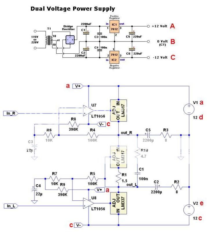
if i were to use dual power supply with +12V 0V -12V how would it be connected to the schematic?
A to a
C to c
what about B?
Thanks in advance
would like to get the layout correct in the continuity between the power supplies and signal grounds as elvee mentioned.
if i were to use dual power supply with +12V 0V -12V how would it be connected to the schematic?
A to a
C to c
what about B?
Thanks in advance
Now your pic is visible, so:hi,
would like to get the layout correct in the continuity between the power supplies and signal grounds as elvee mentioned.
if i were to use dual power supply with +12V 0V -12V how would it be connected to the schematic?
A to a
C to c
what about B?
Thanks in advance
A to a
B to d, e and gnd
C to c
hi all,
Layout changes to address the below:
1) Continuity between the power supplies and signal grounds (note that signal in & out grd is not connected in the layout and uses dual power PSU).
2) Increse heatsink size
3) Added DC/RF filter to the input.
Layout changes to address the below:
1) Continuity between the power supplies and signal grounds (note that signal in & out grd is not connected in the layout and uses dual power PSU).
2) Increse heatsink size
3) Added DC/RF filter to the input.
An externally hosted image should be here but it was not working when we last tested it.
hi all,
Layout changes to address the below:
1) Continuity between the power supplies and signal grounds (note that signal in & out grd is not connected in the layout and uses dual power PSU).
2) Increse heatsink size
3) Added DC/RF filter to the input.
An externally hosted image should be here but it was not working when we last tested it.
I think it is better to put all LM317 on one side, at edge of board, so that people could use their choice of heatsink. Also, the trace width for supplies as well as the output is thin.
Using the supply wires to ensure the integrity of GND connections will most likely bring you problems, like HF oscillations and crosstalk.
Also remember that R2 and R3 are the loads, that's where the signal out connections should be made.
And there is no provision for a local decoupling, that's also likely to cause instabilities.
Also remember that R2 and R3 are the loads, that's where the signal out connections should be made.
And there is no provision for a local decoupling, that's also likely to cause instabilities.
- Home
- Amplifiers
- Chip Amps
- SE class A regulator-chip-amp madness