Hi!
I`ve been working on this type of amplifer for long time and this is the
recent version.
I need some development suggestions.
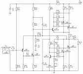
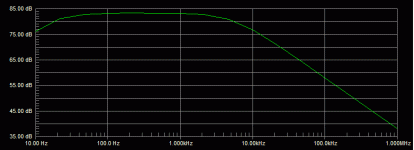
(Open loop gain on the schematic attached is 78dB.)
1.
Mr.John Curl and Mr.Pass always suggesting low open loop gain, but how
to do it? I guess 40dB is ok so how to configure input and vas stage to
acheve low open loop gain? If I remove the bootstrap from the vas, open
loop is then naturaly lower but then THD is much worse and open loop
bandwidth remains the same.Also positive part of sinusoide is clipping.
2. IN the simulation, the amp doesn`t seem to need any type of
compensation. Small (pF) cap across R21 only makes it worse when working
on frquencies higher then 10KHz.Why is that? When 47pF cap is connected
between Q3 gate-drain ,all seems to be ok.
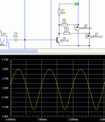
3. Is the open loop bandwidth on the image attached bad as it looks?
I`ve been working on this type of amplifer for long time and this is the
recent version.
I need some development suggestions.
(Open loop gain on the schematic attached is 78dB.)
1.
Mr.John Curl and Mr.Pass always suggesting low open loop gain, but how
to do it? I guess 40dB is ok so how to configure input and vas stage to
acheve low open loop gain? If I remove the bootstrap from the vas, open
loop is then naturaly lower but then THD is much worse and open loop
bandwidth remains the same.Also positive part of sinusoide is clipping.
2. IN the simulation, the amp doesn`t seem to need any type of
compensation. Small (pF) cap across R21 only makes it worse when working
on frquencies higher then 10KHz.Why is that? When 47pF cap is connected
between Q3 gate-drain ,all seems to be ok.
3. Is the open loop bandwidth on the image attached bad as it looks?
Attachments
Bogdan,
This design is sophisticated and will sound very good.
Here is my suggestion.
1. Use heavy local feedback on Q3 by increasing R19 considerably. Start with around 220R.
2. Set up Q8 for A approx 3 with a 1.2K resistor from emitter to ground, and a CCS from the rail to the emitter/emitter resistor. Adjust CCS for appropriate operating point and direct coupling to Q3.
3. Run two 47R resistors in series from the drain of Q2 to the drain of Q7. Then run a 1K collector load of Q1 from the midpoint of these 47R resistors.
It may indeed be possible to get adequate gain from just Q3 alone; keep the bootstrap, it aids linearity, but apply not just source degeneration but possibly also DC feedback from drain back to gate.
This removes global negative feedback entirely, which in turn rids the HF artefacts.
The local FB factor of the hybrid Sziklai pair at the output stage will be very high, and while the intrinsic Zout of Q2/Q7 will be half of 1/S, that is, typically around 200mohm, with even a very conservative fb factor the Zout will be around 50 milliohms.
This sort of amplifier has superb tonal structure, particularly with a tube front end - global feedback tends to destroy the good qualities, and in any case HF response is adequate while Zout is good. You have room to move!
Hope this helps,
Cheers,
Hugh
Thanks AKSA, I was hoping you`ll coment...
I`ll try your suggestions and will reply soon.
CHEERS!
I`ll try your suggestions and will reply soon.
CHEERS!
AKSA said:Here is my suggestion.
1. Use heavy local feedback on Q3 by increasing R19 considerably. Start with around 220R.
I would tend to agree, but won't that considerably limit the output swing? Granted, there may not be a better solution in the end, save for a low S MOSFET, something like a small lateral - too bad they are nearly impossible to get these days 🙁
2. Set up Q8 for A approx 3 with a 1.2K resistor from emitter to ground, and a CCS from the rail to the emitter/emitter resistor. Adjust CCS for appropriate operating point and direct coupling to Q3.
Good idea - make sure it's a 1W resistor as it's a single supply design. Given a 220 ohm R19, you need about 13V on the gate of Q3 for maximum downward swing (you get to within about 8-9V to the ground rail), with Q8 just at the edge of saturation you would need about 14.8mA for the current source. About 3/4 of that goes through the 1.2k resistor.
3. Run two 47R resistors in series from the drain of Q2 to the drain of Q7. Then run a 1K collector load of Q1 from the midpoint of these 47R resistors.
Surely you means 'sources of Q2 and Q7'?
It is a bit odd that the collector load is taken from the sources of Q2 and Q7 as this circumvents the degeneration of Q2 and Q7, which is one way to drop the inner loop gain fo the CFP. Another (more effective one) would be to add an emitter resistor to Q1 (between it's emitter and where it now joins the drains of Q2, Q7 and one side of R3. That is, of course, if you want to do that, as it increases output Z (but it is low to begin with so there might be some room for experimenting here).
It may indeed be possible to get adequate gain from just Q3 alone; keep the bootstrap, it aids linearity, but apply not just source degeneration but possibly also DC feedback from drain back to gate.
This removes global negative feedback entirely, which in turn rids the HF artefacts.
Yes - although, the circuit would benefit from a diode between base of Q1 and + rail. The thing with CFPs is that once the output transistor saturates, the input one has to provide the whole output current. Amongst other problems you may get (check what happens to the Vgs of Q2 and Q7 if the output is shorted or it's driving a very low impedance load!), at this point, if base voltage is not clamped by an external diode, the B-E junction of Q1 will do that job, making base current increase DRAMATICALLY resulting in a rather nasty 'overhang' effect once the output has to get out of saturation - in essence, the output remains stuck to the + rail a while longer than it should. It sounds quite bad.
Normally, this is seldomly recognized since bootstrap 'current sources' have gone out of fashion - a standard current source will generally saturate well before the above can take place. With bootstrapping people tend to forget that it can drive the output signal above the + rail! The diode solution is ot ideal as well (it upsets the voltage in the bootstrap cap, which by definition of the bootstrap effect, should be as constant as possible), but it's the lesser fo two evils.
Regarding other measures to reduce OLG, it is also possible to do this by proportionally increasing R21 and R25. Keep in mind that Q3 is (theoretically0 a voltage driven device, so in essence, for AC the gain of the input stage (Q8) is approximately R20 / (R21 || R25). Increasng proportionally R21 and R25 maintains their ratio, hence keeps GNFB close to constant, but lowers first stage gain. Of course, it also affects the DC operating point of Q8 so R26 and R27 need to be appropriately adjusted. IMHO some form of DC feedback should be retained, makes it so much easyer to account for various DC operating point changes with component tolerances and external influences, and it is not difficult to shunt it for AC whould you want to completely eliminate global NFB for audio frequencies. One way to do this would be to reverse the positions of the load and C5, then use the DC voltage developed on C5 like a sort of 'artificial ground' to set the workpoint of Q8 etc. This also implies a default load as the output would eventually float up to the + rail with no load.
There, that's my $0.02 🙂
Hi Bogdan, Ilimzn,
As so often happens when you post in haste, I made a few errors!! My apologies, good thing this is not a blueprint!
I'll limit my comments to the actual mechanisms, but Q3 is in common source, so only a tiny movement at the gate will drive large voltage output because the device operates in constant current +/-10% owing to the bootstrap.
This brings a virtual high impedance to the drain of Q3, thus the voltage gain of the stage is very large, given by S * Zload; even with a low Z mosfet of 0.1S, and a Zload of 20K (very low figures!) it could be up around 2000, in fact, with commensurate tiny input at the gate.
This is still much higher than needed; so to preserve rail to rail output, we are obliged to use drain/gate resistive feedback, in the manner of NP's original Zen, to pull back the gain to something around 20.
A conventional VAS with 220R degeneration in a run of the mill, Class AB SS amp will not quite swing to the rail, but it's close!
Yes, 1W for a 220R R19 would be appropriate. I make R18/28 current around 17.8mA, with roughly a +/-10% variation rail to rail owing to the bootstrap. This constant current operation is extremely significant to linearity, so resistive feedback across the driver mosfet should be all that is necessary to deliver the lower gain.
Yes, my mistake!
Agree with your comment about taking Q1's collector current from the the bottom of R8/24 rather than the top, at the rail. It negates the degeneration of R8 and R24, which I would like to see at 0R47, in fact.
The use of a small resistor, typically 10R, in the emitter of Q1 will radically reduce OLG, lowering feedback ratio around the loop, improving phase margin and thus promoting stability. However, I can tell you it should not be necessary because I have exhaustive experience in this configuration - bipolar/mosfet CFP - and it's quite stable without it, particularly with a resistive load for the collector of Q1.
Good idea, support this categorically.
As a rule, the stage will catastrophically current limit because of finite current feed through the collector resistor. This produces a sharp spike in positive clipping which only vanishes when the drain of Q7 drops below the base/emitter voltage of Q1. You can improve this situation somewhat by removing DC drive from the base of R28 and driving the base of Q1 through a cap, with base biased through a high value resistor. This works very well, and effectively simplifies the DC coupling issues at the cost of a 100nF cap.
However, clip recovery of this circuit is very good, up there with the best push pull configurations.
I may be wrong, but isn't there a bootstrap action at the feedback node which dynamically increases the effective resistance of R25/21? This would make it tricky to change the emitter load in order to alter the gain of the first stage.
DC feedback is nice to have, yes, but there's not too much need for it if you have a blocking cap on the output!!
I really like the sliding bias scheme on this circuit. I have not tried it myself, but I suspect it would be transparent, and it would greatly improve stability. I have been thinking along these lines myself.......
In closing, I have built something very like this circuit with a 6SL7 front end, capacitively coupled to the base of Q1.
It sounds like a harp in heaven. No global feedback, two 9140s just like yours, Bogdan, and Vcc of 50V. It pulls 28W rms into 8R, sounds like about 100W in full song, and has a Zout of just 38 milliohms.
Keep going. This is a seminal circuit.
Cheers,
Hugh
As so often happens when you post in haste, I made a few errors!! My apologies, good thing this is not a blueprint!
I would tend to agree, but won't that considerably limit the output swing? Granted, there may not be a better solution in the end, save for a low S MOSFET, something like a small lateral - too bad they are nearly impossible to get these days
I'll limit my comments to the actual mechanisms, but Q3 is in common source, so only a tiny movement at the gate will drive large voltage output because the device operates in constant current +/-10% owing to the bootstrap.
This brings a virtual high impedance to the drain of Q3, thus the voltage gain of the stage is very large, given by S * Zload; even with a low Z mosfet of 0.1S, and a Zload of 20K (very low figures!) it could be up around 2000, in fact, with commensurate tiny input at the gate.
This is still much higher than needed; so to preserve rail to rail output, we are obliged to use drain/gate resistive feedback, in the manner of NP's original Zen, to pull back the gain to something around 20.
A conventional VAS with 220R degeneration in a run of the mill, Class AB SS amp will not quite swing to the rail, but it's close!
Good idea - make sure it's a 1W resistor as it's a single supply design. Given a 220 ohm R19, you need about 13V on the gate of Q3 for maximum downward swing (you get to within about 8-9V to the ground rail), with Q8 just at the edge of saturation you would need about 14.8mA for the current source. About 3/4 of that goes through the 1.2k resistor.
Yes, 1W for a 220R R19 would be appropriate. I make R18/28 current around 17.8mA, with roughly a +/-10% variation rail to rail owing to the bootstrap. This constant current operation is extremely significant to linearity, so resistive feedback across the driver mosfet should be all that is necessary to deliver the lower gain.
Surely you means 'sources of Q2 and Q7'? It is a bit odd that the collector load is taken from the sources of Q2 and Q7 as this circumvents the degeneration of Q2 and Q7, which is one way to drop the inner loop gain fo the CFP. Another (more effective one) would be to add an emitter resistor to Q1 (between it's emitter and where it now joins the drains of Q2, Q7 and one side of R3. That is, of course, if you want to do that, as it increases output Z (but it is low to begin with so there might be some room for experimenting here).
Yes, my mistake!
Agree with your comment about taking Q1's collector current from the the bottom of R8/24 rather than the top, at the rail. It negates the degeneration of R8 and R24, which I would like to see at 0R47, in fact.
The use of a small resistor, typically 10R, in the emitter of Q1 will radically reduce OLG, lowering feedback ratio around the loop, improving phase margin and thus promoting stability. However, I can tell you it should not be necessary because I have exhaustive experience in this configuration - bipolar/mosfet CFP - and it's quite stable without it, particularly with a resistive load for the collector of Q1.
Yes - although, the circuit would benefit from a diode between base of Q1 and + rail.
Good idea, support this categorically.
The thing with CFPs is that once the output transistor saturates, the input one has to provide the whole output current.
As a rule, the stage will catastrophically current limit because of finite current feed through the collector resistor. This produces a sharp spike in positive clipping which only vanishes when the drain of Q7 drops below the base/emitter voltage of Q1. You can improve this situation somewhat by removing DC drive from the base of R28 and driving the base of Q1 through a cap, with base biased through a high value resistor. This works very well, and effectively simplifies the DC coupling issues at the cost of a 100nF cap.
However, clip recovery of this circuit is very good, up there with the best push pull configurations.
Regarding other measures to reduce OLG, it is also possible to do this by proportionally increasing R21 and R25. Keep in mind that Q3 is (theoretically0 a voltage driven device, so in essence, for AC the gain of the input stage (Q8) is approximately R20 / (R21 || R25). Increasng proportionally R21 and R25 maintains their ratio, hence keeps GNFB close to constant, but lowers first stage gain. Of course, it also affects the DC operating point of Q8 so R26 and R27 need to be appropriately adjusted. IMHO some form of DC feedback should be retained, makes it so much easyer to account for various DC operating point changes with component tolerances and external influences, and it is not difficult to shunt it for AC whould you want to completely eliminate global NFB for audio frequencies. One way to do this would be to reverse the positions of the load and C5, then use the DC voltage developed on C5 like a sort of 'artificial ground' to set the workpoint of Q8 etc. This also implies a default load as the output would eventually float up to the + rail with no load.
I may be wrong, but isn't there a bootstrap action at the feedback node which dynamically increases the effective resistance of R25/21? This would make it tricky to change the emitter load in order to alter the gain of the first stage.
DC feedback is nice to have, yes, but there's not too much need for it if you have a blocking cap on the output!!
I really like the sliding bias scheme on this circuit. I have not tried it myself, but I suspect it would be transparent, and it would greatly improve stability. I have been thinking along these lines myself.......
In closing, I have built something very like this circuit with a 6SL7 front end, capacitively coupled to the base of Q1.
It sounds like a harp in heaven. No global feedback, two 9140s just like yours, Bogdan, and Vcc of 50V. It pulls 28W rms into 8R, sounds like about 100W in full song, and has a Zout of just 38 milliohms.
Keep going. This is a seminal circuit.
Cheers,
Hugh
Hi!
I tried your suggestions AKSA and ILIMZN (thanks a lot) and everything I
tried gived me strange amp operating on frequencies higher than 10KHz.
I`m not an expert so I`m considering to make it simpler for me.
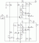
I decided to make a separate power and voltage stage. Voltage amplifier
could be desined with tubes, but I`ll leave it for later...
amp simulation properties:
-Output impedance of attached circuit is 311mOhms.
-Bias set to 2A so output power in 4 Ohms is 30W.
-Dissipation is ~80W per chanell.
-distortion 0.05% 2nd, 0.03% 3rd and 0.02 5th harmonic.
Questions about power stage:
1. Is there any benefit of replacing bias resistor R27 with the current
source (led referenced bjt)?
2. Are there any protection zener diodes needed in this cfp
configuration?
3. Input impedance is now set to ~44K. What could be the optimum value
of the input impedance for this kind of amplifier.
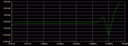
4.I also attached the image of circuit bandwidth and as you can see
there is a problem. What is the cause of this? Is there any kind of
compensation needed?
Any other suggestions are welcome.
Cheers!
I tried your suggestions AKSA and ILIMZN (thanks a lot) and everything I
tried gived me strange amp operating on frequencies higher than 10KHz.
I`m not an expert so I`m considering to make it simpler for me.
I decided to make a separate power and voltage stage. Voltage amplifier
could be desined with tubes, but I`ll leave it for later...
amp simulation properties:
-Output impedance of attached circuit is 311mOhms.
-Bias set to 2A so output power in 4 Ohms is 30W.
-Dissipation is ~80W per chanell.
-distortion 0.05% 2nd, 0.03% 3rd and 0.02 5th harmonic.
Questions about power stage:
1. Is there any benefit of replacing bias resistor R27 with the current
source (led referenced bjt)?
2. Are there any protection zener diodes needed in this cfp
configuration?
3. Input impedance is now set to ~44K. What could be the optimum value
of the input impedance for this kind of amplifier.
4.I also attached the image of circuit bandwidth and as you can see
there is a problem. What is the cause of this? Is there any kind of
compensation needed?
Any other suggestions are welcome.
Cheers!
Attachments
Hi Bogdan,
Your simulation is showing HF problems, which are either coming from the collector drive arrangement on Q1, or the sliding bias configuration operating through C1.
To verify this, try:
#1 Remove R16 and R7 entirely; change R29 to 680R, and connect the top to the junction of R2 and R14. This exploits the degeneration of R8 and R24, reducing OLG and thus improving phase margin.
Now run the simulation. Is the problem still evident? If yes, proceed to the next step below.
#2 Increase R22 to 22K.
Run simulation. Any different? If the problem is resolved, then remove C1 and connect the top of R22, now 22K, to the drain of Q6/Q4. This will stabilise the DC operating point better, and improve bias sliding at very low frequencies where the bass amplititude is high.
#3 Since the sliding bias requires a modulation of the gate voltages at Q6 and Q4, use a very low impedance emitter follower to drive these high capacitance gates. This will also reduce current draw of the variable CS control circuits some four times. Just add Q6B, a PNP TO92 bipolar, with its emitter fed from a 3K3 which is connected to the junction of R1 (change to 10K) and R2 (change to 3K3). The two 220R gate stoppers are now driven directly from the emitter of Q6B; while the collector is taken straight to ground. Q6B's base is directly connected to the collector of Q6. Q6, the control device, will pass 1.65mA, while Q6B will pass 4.85mA, giving it a source impedance of 5.4 ohms at 20C. This would give very low source impedance to drive those gates. Gates should be shaken, not stirred......
Hope this helps,
Cheers,
Hugh
reducing R29 to higher value resolves the problem. Now it`s all ok.
Once again, Is there any benefit of replacing bias resistor R27 with the current
source (led referenced bjt) and wath would be the optimum value for the input impedance?
While I construct pcb for a power stage, it would be good for me to think of voltage amplifer stage. I`ll reply soon with my idea.
Voltage amp should have 16V peak to peak output for maximum power at 4 ohms.
bogdan_borko said:reducing R29 to higher value resolves the problem. Now it`s all ok.
Once again, Is there any benefit of replacing bias resistor R27 with the current
source (led referenced bjt) and wath would be the optimum value for the input impedance?
Yes, replacing R27 with a constant current source will improve the amplifiers PSU rejection. There is no optimal value of input impedance; it just has to be high enough to not load the preamp excessively. Anything above 20k or so should be more than enough for most applications.
A simpler option would be to split R27 into two series-connected resistors, say a pair of 27k's with the junction of the two resistors bypassed to ground with a large electrolytic capacitor; say 220-470uF.
If you choose to use a LED biased CCS, used a trimpot in series with the emitter resistor so that the biasing current can be varied so that the amplifiers DC operating point can be set accurately to the optimal value.
Cheers,
Glen
AKSA said:Hi Bogdan, Ilimzn,
As so often happens when you post in haste, I made a few errors!! My apologies, good thing this is not a blueprint!
Ah, well, I am at least equally guilty of this 🙂
I'll limit my comments to the actual mechanisms, but Q3 is in common source, so only a tiny movement at the gate will drive large voltage output because the device operates in constant current +/-10% owing to the bootstrap.
This brings a virtual high impedance to the drain of Q3, thus the voltage gain of the stage is very large...
This is still much higher than needed; so to preserve rail to rail output, we are obliged to use drain/gate resistive feedback...
A conventional VAS with 220R degeneration in a run of the mill, Class AB SS amp will not quite swing to the rail, but it's close!
Yes, that is of course right, and I made a rather obvious error in calculation (today seems not to be one of my better days 😉 ). Even so, given that the drain resistors of Q3 are 2x560 ohms and the source is 220 ohms, and the current through D/S is defined by D having to be near Vcc/2 DC potential, it follows that this is about
17.8mA current, which in turn makes a 3.92V drop on R19, and this is the part of the swing you lose off the ground rail even if the VAS load impedance was infinite. The point being, that while increasing R19, there is a point where this loss will get signifficant.
Agree with your comment about taking Q1's collector current from the the bottom of R8/24 rather than the top, at the rail. It negates the degeneration of R8 and R24, which I would like to see at 0R47, in fact.
Agreed - current sharing will be better, amongst other things.
However, I can tell you it should not be necessary because I have exhaustive experience in this configuration - bipolar/mosfet CFP - and it's quite stable without it, particularly with a resistive load for the collector of Q1.
This is very nice to know as i am using a BJT/MOS CFP in a design i am developing as well, and so far my experience is the same - but as you have much more experience with this, it is a nice corroboration of my own choice to use it - thanks.
I may be wrong, but isn't there a bootstrap action at the feedback node which dynamically increases the effective resistance of R25/21? This would make it tricky to change the emitter load in order to alter the gain of the first stage.
I see what you mean but I probably did not express myself right - if we were talking OLG, then, in order to keep all other things equal, the end of R21 that is, in closed loop operation, connected to the output, would be connected to AC ground, then what I wrote becomes apparent. In closed loop operation it is somewhat tricky to define anything but effective gain of the first stage.
DC feedback is nice to have, yes, but there's not too much need for it if you have a blocking cap on the output!!
True, as long as you also have sufficiently low open loop gain, or, in fact, so low you operate the amp open loop (i.e. no GNFB). Then, actual current gains, gm's and Vgs treshold tolerances are insignifficant compared to static conditions set by passive components. A volt or two departure from ideal DC voltage on the output in front of the coupling cap will certainly be no problem.
As it was originally drawn, the amp is almost a complete anti-thesis to that, and DC feedback is mandatory. Somewhere inbetween are the cases where you can get a few volts drift, so DC feedback is something to consider.
In closing, I have built something very like this circuit with a 6SL7 front end, capacitively coupled to the base of Q1.
It sounds like a harp in heaven. No global feedback, two 9140s just like yours, Bogdan, and Vcc of 50V. It pulls 28W rms into 8R, sounds like about 100W in full song, and has a Zout of just 38 milliohms.
Briliant, especially with a 6SL7, it suggests that the actual input impedance of the CFP output stage is very high - again something my recent experiments have shown, although in my case the output is complementary.
Hi Ilimzn,
Zin of a cap coupled base is, by my empirical guestimates, around 200K, and dominated by the collector impedance of the driver.
Keep going. This is a rewarding configuration.......
Cheers,
Hugh
Zin of a cap coupled base is, by my empirical guestimates, around 200K, and dominated by the collector impedance of the driver.
Keep going. This is a rewarding configuration.......
Cheers,
Hugh
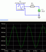
4.On the attached picture you can see Ugd charging resulting capacaty of two IRFP9140 mosfets Cgd is 320pF. You can see the charging current is 3.3mA peak.
If we do not consider that Cgs and Cgd is changing with the operating conditions of the mosfet, then we can calculate that the minimum gate charging current fot this cfp at 100KHz is:
Ig= I_Cgs+I_Cgd=0.6mA + 3.3mA= 3.9mA
AM I THINKING RIGHT?
javascript:smilie(' ')
')
If we do not consider that Cgs and Cgd is changing with the operating conditions of the mosfet, then we can calculate that the minimum gate charging current fot this cfp at 100KHz is:
Ig= I_Cgs+I_Cgd=0.6mA + 3.3mA= 3.9mA
AM I THINKING RIGHT?
javascript:smilie('
')Attachments
Yes, Bodgan,
You are right to consider the capacitance of the gate highest in this configuration, but fortunately the voltage swing wrt rail is not high, so slew rate is still limited.
I have set mine at 4.2mA, which gives 3dB down at 75KHz.
Close enough for government work......
Cheers,
Hugh
You are right to consider the capacitance of the gate highest in this configuration, but fortunately the voltage swing wrt rail is not high, so slew rate is still limited.
I have set mine at 4.2mA, which gives 3dB down at 75KHz.
Close enough for government work......
Cheers,
Hugh
- Status
- Not open for further replies.
- Home
- Amplifiers
- Solid State
- SE Class-A developing