I just did a reading and had only 0.8mv on one and 1.0mV on the other channel and only after letting it play for a while, at first I just had 0 on both channels. Can this be due to the resistor that is in place instead of the pot that just has a too high value or is there something else going on ?
You've removed the shorting wire from across the vbe multiplier 😉 (had to ask).
Yes, its possible the bias is wrong due to the different characteristics of the replacement transistors. All you need do is remove the resistor and fit a 10k pot, but you must start with the pot on 10k and work down from there.
(I mentioned 10k but seeing as you have very low bias with the 3.9k fitted (make sure it is 3.9k) then you could use a 4.7k pot and get better resolution. Again, start with it at 4.7k and work down)
If you can not get the bias correct with a pot then we might have to look at slightly modifying the vbe generator.
Okay, sounds like a plan. I don't know if I will be able to to this by the end of the week but as soon as I have something I'll post.
And yes I removed the shorting wire from the vbe multiplier 😎
And yes I removed the shorting wire from the vbe multiplier 😎
OK, just remember to use the bulb tester initially, and then when you are happy its OK, turn the bias back down, remove the bulb and then set it up for real.
I'm not exactly sure how to install the pot because I have now two resistors at that spot, whereas the schematics only show one (the 3.9k) and a set of diodes but no pot.
I went looking for some pictures on the internet but not much there, I found two that had a pot installed but both of them were different in the components surrounding it.
here it is as it's now (well before changing the fault components).

I went looking for some pictures on the internet but not much there, I found two that had a pot installed but both of them were different in the components surrounding it.
here it is as it's now (well before changing the fault components).
That sounds even better actually because the two diodes were a weird arrangement. You need to identify the two resistors and their values and then replace the lower one that connects across base and emitter of the vbe multiplier with a preset. Use a value higher than the fitted resistor (next value up)
Attachments
I just noticed that on the circuit board in the service manual the pins of the vbe multiplier are B, C, E (2sc372) but on the actual board it says C, B, E which doesn't correspond to the way the transistor is put in, how can it still work if it is in the wrong way ? I hope this is comprehensible 😱
Also the resistor between the base and emitter has a value of 480ohm, nothing near 3.9k !
Also the resistor between the base and emitter has a value of 480ohm, nothing near 3.9k !
Last edited:
You need to confirm by measurement (continuity) that the collector really does go to the 'top' driver and the emitter to the 'lower' driver. The circuit diagram is correctly drawn as regards the transistor connections. Printing on boards can sometimes be in error... confirm by measurement. The middle leg would normally be the collector for a T098 package.
The indications on the board seem to be the right ones, with continuity test the base of the transistor (c on the board) goes to the "top" driver and the emitter (also e on the board goes to the "lower" driver. so the collector and base of the vbe multiplier transistor should be switched. Could this be why I only had 0.7mV across the 0.27ohm resistor ? Initially the vbe multiplier was a motorola transistor which might have had a different pin out.
yes it is but this picture is from when i first opened it, all the components circled in red have been replaced.
The indications on the board seem to be the right ones, with continuity test the base of the transistor (c on the board) goes to the "top" driver and the emitter (also e on the board goes to the "lower" driver. so the collector and base of the vbe multiplier transistor should be switched. Could this be why I only had 0.7mV across the 0.27ohm resistor ? Initially the vbe multiplier was a motorola transistor which might have had a different pin out.
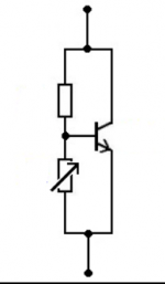
Collector should go to the top driver. Like this,
Attachments

Yes that is what I thought also which means that the vbe multiplier is wrongly installed it's B that is going to the top driver as it is now. What I was wondering is could this be the cause for the bias to be at 0.7mV (the manual says 0.2 mA, do I convert this into mV by multiplying it by 0.27 ohm ? )
You need to be very very clear on what we mean by bias (current).
It is a steady current that flows in the two output transistors and is needed to minimise crossover distortion. The current can be deduced by measuring the volt drop across either of the 0.27 ohms. The same current flows in each.
Typically we might be looking at anywhere up to 100 milliamps (or even more) as a theoretical optimum but other factors come into play such as heatsink size and how much ventilation there is to get rid of the heat. So you need to know the manufacturers recommended figure and aim for that.
Ohms law which is V=I*R allows you to calculate any of three variables by knowing the other two.
I=V/R and R=V/I
You mentioned 12 milliamps earlier. That means a voltage of 0.012*0.27 which is 3.2 millivolts should appear across each 0.27 ohm.
Yes that is what I thought also which means that the vbe multiplier is wrongly installed it's B that is going to the top driver as it is now. What I was wondering is could this be the cause for the bias to be at 0.7mV (the manual says 0.2 mA, do I convert this into mV by multiplying it by 0.27 ohm ? )
The transistor on your circuit diagram is correctly drawn. So the middle leg (I looked up the pin outs of the of the 2SC372) of the vbe multiplier should go to the collector of Q803, the collector of Q801 and the base of Q807. All as drawn on the diagram.
Remember you are measuring across the 0.27 ohms for voltage and that is done with no speakers attached
This is exactly why I am here, learning, as a matter of fact I new these few things but it is always nice to have it explained again so clearly.
I don't always have the right terms in english which might be confusing sometimes. I was wrong when I said 12mA, this was actually the calibration of the multimeter, here is a pic from the manual :

This would mean 0.54mV.
On The other Scott A426 I had a reading that was steadily increasing up to way over 40mV.
I don't always have the right terms in english which might be confusing sometimes. I was wrong when I said 12mA, this was actually the calibration of the multimeter, here is a pic from the manual :
This would mean 0.54mV.
On The other Scott A426 I had a reading that was steadily increasing up to way over 40mV.
0.2ma sounds an implausible value to be honest. Its way to low.
The 40mv on your other amp sounds a bit to high... and to see it increasing over time is actually normal up to a point but it should settle and stabilise as the heatsink warms. Ideally, in a well designed amp the bias should be fairly constant from switch on through to the amp being really hot from working hard. We may never achieve that with this design but it needs at least 10 to 20 milliamps to reduce distortion to acceptable levels.
I think you need to configure the transistor so it as drawn on the diagram and in the little image I posted earlier, together with a preset to alter the bias. Lets see how it sets up and how stable it is. Always use the bulb tester though.
The transistor type isn't critical as long as it can be in thermal contact with the heatsink.
Back later 🙂
The transistor on your circuit diagram is correctly drawn. So the middle leg (I looked up the pin outs of the of the 2SC372) of the vbe multiplier should go to the collector of Q803, the collector of Q801 and the base of Q807. All as drawn on the diagram.
On the board it's the collector of the vbe that goes to these three other transistors so I will have to cross its base and collector.
On the board it's the collector of the vbe that goes to these three other transistors so I will have to cross its base and collector.
I'm not quite following you on that. It is collector that goes to those three transistors. Do you mean that this point then doesn't go to the collector of the vbe multiplier transistor ?
- Home
- Amplifiers
- Solid State
- Scott A 426