
haha!
If parralleling output devices could affect the free running frequency of the amp. I want to drive lower resistance, like 2 ohm if possible (assuming that i have the proper power supply)
thanks.
If parralleling output devices could affect the free running frequency of the amp. I want to drive lower resistance, like 2 ohm if possible (assuming that i have the proper power supply)
thanks.
Sorry about asking something that is in the document. I read it some months ago and I didn't remember that detail, only the schematics.
About paralleling, I think the only influence in the running freq. could be due to increased gate charge/capacitance, so slower turns on/off. The mosfets used by IR have very low gate charge, btw. I can't figure out another way in that they affect sw. frequency. The influence shouldn't be very large, I guess.
Regards,
Pierre
Considering layout, using more robust FETs would be easier. Specially considering that you could lower the switching frequency because you use the amp only for a subwoofer.
Regards
Charles
Regards
Charles
Concerning driving lower impedance loads:
Would the feedback network suffice?
The feedback and load impedance are largely independant of each other.
For the lower impedance the output filter would have to be redesigned however.
And if he really wants to use a slower switching frequency the feedback has to be changed accordingly.
IMO it is still wise to try it first as it is and then start to modify, unless you'd like to debug different issues at once of course !
Regards
Charles
Hi,
I agree that's too big a hassle/risk to take before getting it working and debugged at all, but it is nice to know what lays ahead.
Thanks for that.
I agree that's too big a hassle/risk to take before getting it working and debugged at all, but it is nice to know what lays ahead.
Thanks for that.
You all feels like International rectifier have done a bad job.  and that it have to work bad
C'mon, lets get optimistics. 😀
and that it have to work bad C'mon, lets get optimistics. 😀
I don't feel like that but you might have to fiddle anyway to get it working properly unless you take the original PCB layout.
Regards
Charles
Regards
Charles
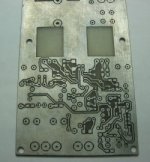
Hi, here is my PCB, i finaly found few minutes to do it.
I do pcb artwork for RF transmitters, as well as the design of them, so i cant mess that much with that. I am no beginner.
BTW, i managed to get the updated service manual for the PB 12, there is a lot of rework, more than one could think of
Since i go to the CES often, i got good contacts 😀
I do pcb artwork for RF transmitters, as well as the design of them, so i cant mess that much with that. I am no beginner.
BTW, i managed to get the updated service manual for the PB 12, there is a lot of rework, more than one could think of
Since i go to the CES often, i got good contacts 😀
Attachments
Well..... get stuffed..... I mean.... 🙂
Look forward to the results, far as I know no one here has tried it, but some had shown interest in it awhile back.
Look forward to the results, far as I know no one here has tried it, but some had shown interest in it awhile back.
Post #119 UcD 180 thread.
http://www.diyaudio.com/forums/showthread.php?postid=458949#post458949
"Not only bad designs have overshoot... Good designs delivering 30A also produce overshoot. Think of it: 10...20nH circuit inductance, 30A current... No way you can stop that from overshooting, apart from using these fancy top-cooled SMD fets (e.g. IR DirectFET). Ringing is a different affair. If you have it (ie when using through-hole packages) snubbers do magic.
I've been talking to MOSFET designers about operating FETs in avalanche like this. Having properly analysed the whole thing we agreed there's nothing to worry about.
Cheers,
Bruno"
That what you had in mind Charles? Google isn't cutting it these days. Run searches for what you know is there and it turns up useless results, or more commonly nothing. (keyphrase site:wwwdiyaudio.com) not so useful anymore. Try it "Ringing is a different affair site:www.diyaudio.com" three hits and non on target.. Huh.. Guess I'll stop wasting my time with that little non feature.
1.) Yes it was that statement from Bruno
2.) Pat's PCB looks cool. BTW: Knowledge in RF layouting is always a good thing when it comes to class-d amps.
Regards
Charles
2.) Pat's PCB looks cool. BTW: Knowledge in RF layouting is always a good thing when it comes to class-d amps.
Regards
Charles
Hi, can someone explain me the snubber thing, and the overshoot thing too?
There is an option on the original board for a cap at the input of the op amp. ?? limit the bandwidht?
thanks.
There is an option on the original board for a cap at the input of the op amp. ?? limit the bandwidht?
thanks.
In the simplest form snubbers are series RC circuits placed from source to drain (across) the mosfet, with the intention of damping ringing of the square waveform. I think another variation of it is an RCD circuit.
A cap on the input is a "trick" which is often a kind of haywire fix.
One purpose it serves is to slow the charging of the gate, and another is possibly to help reduce "gate step" due to high dv/dt transients, by making gate source capaticance much larger than the miller/gate drain capacitance, less voltage builds up at the gate. I'm not really sure how effective that would actually be though, because you have both gate inductance and resistance in there as well.
How is it comming along?
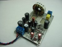
wow, thats was quick...it is 99% complete, i have to machine the heat sink, and find a proper pnp transistor, i only have mmbt3906 where is it only 40v ceo...
thanks for the inputs.
thanks for the inputs.
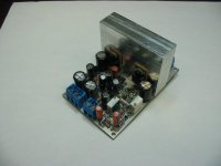
ok, one word: it works.
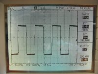
question tough...the bias adjustment of the op amp dont seems to change a thing, i tough i could be able to adjust the output of the amp, but it just operates at 0-5v triangle wave, no matter how it is set...so, what does it affect in this application??
The free running frequency is 395mhz...
question tough...the bias adjustment of the op amp dont seems to change a thing, i tough i could be able to adjust the output of the amp, but it just operates at 0-5v triangle wave, no matter how it is set...so, what does it affect in this application??
The free running frequency is 395mhz...
Attachments
- Status
- Not open for further replies.
- Home
- Amplifiers
- Class D
- schematic of my future D amp for the pb12