I have been toying with the BA3 circuit, tying to overcome the level shifter need to bias the output stage and was wondering if it would possible or even good idea to try to do so using a Scahde type toplogy. In all the version I have seen, it is done on the input stage and the feedback is returned to the midpoint between the gate and a large value gate resistor. If this is a necessary element, how will it affect the operation of the circuit having this large value resistor in the gate of the mosfet, considering that it is being fec by the Jfet input stage.
Attachments
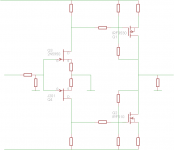
I assume (poor PSRR) is due to the fact that the bias net is tied to the rails.
Not really. The drain loads in the first stage are resistors instead of current sources, so the ac signal voltage at the drain is (Vrailnoise - (gm x vin x rdrain)). Every 1 millivolt of supply rail noise becomes 1 millivolt of input voltage to the second stage, so the PSRR is 20 x log10(1 / 1) = 0 dB. And PSRR=0dB is rather poor.
Inadvertent schematic error in front end; same gender N-JFEts which need to be complementary.I have been toying with the BA3 circuit, tying to overcome the level shifter need to bias the output stage and was wondering if it would possible or even good idea to try to do so using a Scahde type toplogy. In all the version I have seen, it is done on the input stage and the feedback is returned to the midpoint between the gate and a large value gate resistor. If this is a necessary element, how will it affect the operation of the circuit having this large value resistor in the gate of the mosfet, considering that it is being fec by the Jfet input stage.
Program didn't have P channel Jfets in standard library. From what I have learned, the poor psrr is a result of the bias net being tied to the output. In both F5 and BA3 the level shifter helps in this regard.
Use a regulated PSU for BA3FE also, so as to enable you to compare its performance with that of your circuit.Program didn't have P channel Jfets in standard library. From what I have learned, the poor psrr is a result of the bias net being tied to the output. In both F5 and BA3 the level shifter helps in this regard.
I currently listening to it with reg from balanced zen line stage. Being an experiment for FE of power amp, regulator gets complicated. If run balanced, I believe it will be OK, but a regular may be worthwhile.
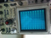
Name that Waveform
As the title of the post suggest, I need some help. Getting this out of a proto pre. THis is a 1K sine wave.
As the title of the post suggest, I need some help. Getting this out of a proto pre. THis is a 1K sine wave.
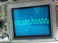
Probably you have already sorted this but looks like the input devices in the bad channel need attention
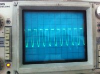
Nice and cheerful new avatar.Oops. Figured it out. Have a bad transistor somewhere. Here is opposite channel. First two is bad channel. Second two are the good one.
- Status
- Not open for further replies.
- Home
- Amplifiers
- Pass Labs
- Schaded VAS