I'm going to say...
First prove to yourself that the good channel only has around 0.65 volts across base and emitter of the outputs. In other words that the good channel behaves as expected.
I'm wondering if the circuit is unstable (oscillating at HF or RF) as that would give totally misleading voltage readings. If any of the drivers or outputs are modern parts and not original then that could cause instability because they are faster and made using different processes.
Is the Zobel network OK. Resistor OK? That is the 10 ohm 5 watt resistor and series 0.047uF cap on the output. Is there any voltage across that resistor at all when checked on AC and DC ranges on your meter. If there is then its oscillating.
Ideally you should check with a scope to make sure it is OK.
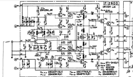
It might be worth pursuing the stability theory but I would have to see a full circuit to see if anything could be altered easily.

First prove to yourself that the good channel only has around 0.65 volts across base and emitter of the outputs. In other words that the good channel behaves as expected.
I'm wondering if the circuit is unstable (oscillating at HF or RF) as that would give totally misleading voltage readings. If any of the drivers or outputs are modern parts and not original then that could cause instability because they are faster and made using different processes.
Is the Zobel network OK. Resistor OK? That is the 10 ohm 5 watt resistor and series 0.047uF cap on the output. Is there any voltage across that resistor at all when checked on AC and DC ranges on your meter. If there is then its oscillating.
Ideally you should check with a scope to make sure it is OK.
It might be worth pursuing the stability theory but I would have to see a full circuit to see if anything could be altered easily.
Testing B-E in the good channel shows 10mv of bias at around .55v across B-E. As I increase the bias adjustment it does rise close to .65 but bias got very high and momentarily tripped the protection so I backed it off.
The New drivers are the same as running in the good channel. The only other new transistors are on the amp driver card (I guess these are pre drivers) TR2-5 (Orig 2sc1775) replaced with KSC1845 and TR6-9 (Orig 2sa872) replaced with KSA992.
The 10 ohm resistors show 0V AC and DC (There was a few mV DC but I adjusted the offset to 0 and it is now 0). I had to pull one leg of the .047 uf caps to test but they test ok with infinite resistance and show the correct capacitance.
I do have an analog scope and did not see any ripple on either side of these resistors.
(When the bias pot failed some time ago and the bias was able to rise I did see an oscillating current draw while watching the dim bulb. I'm not sure this helps at all.)
Attachments
Thanks for the diagram.
That's exactly as it should be. Remember the B/E junction behaves a lot like a diode and so it should not be able to support a highish voltage across it. The voltage should limit out at perhaps 800mv if you were pushing lots and lots of current through it.
This is why I said the theory won't fail us. If you are seeing a volt or more over the B/E junction then something isn't how it seems.
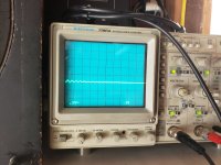
So with the scope grounded to chassis you are saying the 1.2 volts DC is clean when measured on R39 and R40 (the 4.7 ohm that goes to the base of the outputs)? The scope trace should be a thin clean line (no signal of any kind). Use AC coupling on the scope and make sure you are using something like 100mv/div sensitivity.
I'm out of time for today 🙂
Testing B-E in the good channel shows 10mv of bias at around .55v across B-E. As I increase the bias adjustment it does rise close to .65 but bias got very high and momentarily tripped the protection so I backed it off.
That's exactly as it should be. Remember the B/E junction behaves a lot like a diode and so it should not be able to support a highish voltage across it. The voltage should limit out at perhaps 800mv if you were pushing lots and lots of current through it.
This is why I said the theory won't fail us. If you are seeing a volt or more over the B/E junction then something isn't how it seems.
So with the scope grounded to chassis you are saying the 1.2 volts DC is clean when measured on R39 and R40 (the 4.7 ohm that goes to the base of the outputs)? The scope trace should be a thin clean line (no signal of any kind). Use AC coupling on the scope and make sure you are using something like 100mv/div sensitivity.
I'm out of time for today 🙂

This is the waveform I am seeing when clipped to either the r39/40 4.7 ohm resistors leading to the base of the outputs. This looks the same on the good and faulty channel.
I just want to say thank you for holding my hand through this and helping me try to figure this one out. I really do appreciate it and feel like ive learned quite a bit walking through the steps you laid out..
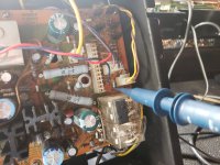
Ive fixed a lot of amps over the past few years and this one has really eluded me. I've been working on it off and on since about November. Basically just stuck on this one issue.
I just want to say thank you for holding my hand through this and helping me try to figure this one out. I really do appreciate it and feel like ive learned quite a bit walking through the steps you laid out..
Ive fixed a lot of amps over the past few years and this one has really eluded me. I've been working on it off and on since about November. Basically just stuck on this one issue.
Attachments
You're not the only one 🙂Basically just stuck on this one issue.
You're very welcome, ones like this are interesting.I just want to say thank you for holding my hand through this and helping me try to figure this one out.
Lets break it down to just one pair of output transistors (the amp would work with just one pair anyway, the three in parallel are just to increase the current handling)
You need to check this methodically. Do not assume anything as being correct. Measure it and prove it. This is very important if the amp has an unknown history. For example have the leads to the board with the output transistors had the connections to the base and emitters reversed... sounds mad but check it. Prove it.
So taking one pair of outputs and it doesn't matter which you place your meter negative lead on the junction of the 0.33 ohms for that pair. That is our reference point.
Now measure the on the collectors of that pair from that reference point and prove you have the supply voltage present and correct on both.
This shows the idea. The voltages sources on the left are your measured -/+1.2 volts. You can see how that turns the outputs fully on and generates a massive bias current. Note how the base/emitter junctions levels out at around 700 millivolts. It can not go higher for a silicon transistor.
In the simulation look at the voltage difference across the 4.7 ohms. You can see just how much base current is flowing,
If these conditions are met then the output pair must conduct.
Prove by measurement that the base and emitter connections (the wires between the boards) are correct and not reversed.