Hello everyone,
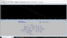
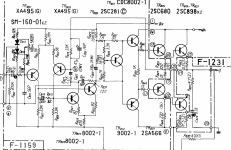
I made an attempt to re-create the main amplifier circuit from a vintage Sansui AU-999 integrated amp. I'm planning to eventually create a clone of the driver PCB in KiCAD and experiment with maybe somehow improving the amp's performance.
I don't have a massive experience with LTspice and circuit design in general and as a first step, I would for someone to verify the simulation.
At this point, I can get decent performance out of the amp at 1khz, with 0.00x DC offset and 0.02% THD but as the frequency goes up the performance degrades massively.
There seem to be excessive amounts of crossover distortion, especially from 10khz and above, the DC offset also rises to an unacceptable level.
The simulation is set up for THD calculation using the .four command
I used a couple of external libraries (included in the zip file)
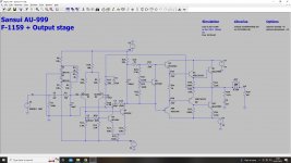
MJ15003 as output devices
MJE15032/3 as drivers
BC560s as a differential input pair
Bias is set at ~33mA
I changed some of the small capacitor values to improve stability (at least what I thought I was doing when referring to bode plots)
All files are attached in the zip file
Any input/feedback would be much appreciated
I made an attempt to re-create the main amplifier circuit from a vintage Sansui AU-999 integrated amp. I'm planning to eventually create a clone of the driver PCB in KiCAD and experiment with maybe somehow improving the amp's performance.
I don't have a massive experience with LTspice and circuit design in general and as a first step, I would for someone to verify the simulation.
At this point, I can get decent performance out of the amp at 1khz, with 0.00x DC offset and 0.02% THD but as the frequency goes up the performance degrades massively.
There seem to be excessive amounts of crossover distortion, especially from 10khz and above, the DC offset also rises to an unacceptable level.
The simulation is set up for THD calculation using the .four command
I used a couple of external libraries (included in the zip file)
MJ15003 as output devices
MJE15032/3 as drivers
BC560s as a differential input pair
Bias is set at ~33mA
I changed some of the small capacitor values to improve stability (at least what I thought I was doing when referring to bode plots)
All files are attached in the zip file
Any input/feedback would be much appreciated
Attachments
Last edited:

One comment, you don't get a realistic idea of the offset voltage because the input transistors are identical.
Hi tommost,One comment, you don't get a realistic idea of the offset voltage because the input transistors are identical.
Thanks for your reply.
The differential input pair will be matched when I get to build the boards. The DC offset is controlled by R4-R5, which in the real circuit is done with a trimpot.
R21-R22 is also a trimpot for the bias adjustment.
I'm just unsure what is causing this excessive distortion at higher frequencies. Even at 1kHz the crossover distortion is clearly visible when you look at the waveform.
Regards
You need more bias from the Vbe multiplier. I increased R20 to 4.7K as a guess and the distortion seems to have gone away. You should experiment with the proper values.Hi tommost,
Thanks for your reply.
The differential input pair will be matched when I get to build the boards. The DC offset is controlled by R4-R5, which in the real circuit is done with a trimpot.
R21-R22 is also a trimpot for the bias adjustment.
I'm just unsure what is causing this excessive distortion at higher frequencies. Even at 1kHz the crossover distortion is clearly visible when you look at the waveform.
Regards
I biased the output stage as per the original Sansui AU-999 service manual at 33mA.
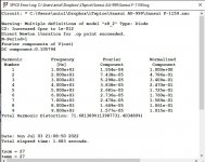
I did try raising the value of R20 to 4k7 but I'm still getting(with 10kHz sine input):
Fourier components of V(out)
DC component:0.112407
Harmonic Frequency Fourier Normalized Phase Normalized
Number [Hz] Component Component [degree] Phase [deg]
1 1.000e+03 1.491e-04 1.000e+00 -172.01° 0.00°
2 2.000e+03 8.859e-05 5.943e-01 -162.62° 9.39°
3 3.000e+03 1.303e-04 8.739e-01 -144.41° 27.60°
4 4.000e+03 2.821e-05 1.892e-01 114.43° 286.44°
5 5.000e+03 2.903e-05 1.947e-01 165.76° 337.77°
6 6.000e+03 5.273e-05 3.537e-01 170.82° 342.83°
7 7.000e+03 7.445e-05 4.994e-01 -21.02° 150.99°
8 8.000e+03 1.638e-05 1.099e-01 -49.72° 122.29°
9 9.000e+03 1.258e-05 8.439e-02 -75.29° 96.72°
Total Harmonic Distortion: 125.873411%(14585051.907895%)
I couldn't see any crossover with the 4.7K. I didn't look at the FFT.I biased the output stage as per the original Sansui AU-999 service manual at 33mA.
I did try raising the value of R20 to 4k7 but I'm still getting(with 10kHz sine input):
Fourier components of V(out)
DC component:0.112407
Harmonic Frequency Fourier Normalized Phase Normalized
Number [Hz] Component Component [degree] Phase [deg]
1 1.000e+03 1.491e-04 1.000e+00 -172.01° 0.00°
2 2.000e+03 8.859e-05 5.943e-01 -162.62° 9.39°
3 3.000e+03 1.303e-04 8.739e-01 -144.41° 27.60°
4 4.000e+03 2.821e-05 1.892e-01 114.43° 286.44°
5 5.000e+03 2.903e-05 1.947e-01 165.76° 337.77°
6 6.000e+03 5.273e-05 3.537e-01 170.82° 342.83°
7 7.000e+03 7.445e-05 4.994e-01 -21.02° 150.99°
8 8.000e+03 1.638e-05 1.099e-01 -49.72° 122.29°
9 9.000e+03 1.258e-05 8.439e-02 -75.29° 96.72°
Total Harmonic Distortion: 125.873411%(14585051.907895%)
Visually, the waveform looks cleaner, however, the log still gives me an unacceptable THD figure.I couldn't see any crossover with the 4.7K. I didn't look at the FFT.
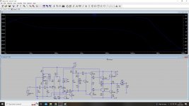
What I actually found is that the input signal into Q1 has already an element of the x-over distortion.
The only thing I can think of is that the DC compensation is somehow affecting the signal?
Looking at the R4/R5 junction which I guess is your offset trimpot, I see about 55 mV of the output signal there. As a wild a$$ guess I placed a 10 uF cap across each of D1 and D2, and another from the R3/R4/R5 junction to ground. This lowered the AC component there to about 75 uV. I used perfect caps and made no attempt to optimize the values so some work remains there.
Here's the output FFT from the circuit you uploaded:

With the DC offset caps added and R20 = 4.7K this is what it looks like:

There's no denying the revised circuit is a lot cleaner. But for some reason the THD figures don't reflect it, I don't know why.
Here's the output FFT from the circuit you uploaded:
With the DC offset caps added and R20 = 4.7K this is what it looks like:
There's no denying the revised circuit is a lot cleaner. But for some reason the THD figures don't reflect it, I don't know why.
Thanks for taking the time to look into this @tommost,
Yes, I can re-create your results by solely increasing the bias, however, I'm not sure whether the amp would take 880mA of bias (33mA is the original value)
I just think there maybe is an error in one of my models? Saying that I changed all transistor models to perfect npn/pnp and I'm still getting very high THD from my log file.
Looking at this some more my Vbe multiplier values placed the bias at almost 900 mA which is probably not practical. But the original values gave about 33 mA on Q9 but only 16 mA on Q10 which is apparently not enough. I'm getting ready to leave for the day so this will have to wait for a bit but I never did like quasi complementary outputs, I suspect that's the root cause of the asymmetry.
EDIT you beat me to it by 1 minute lol.
EDIT you beat me to it by 1 minute lol.
Thanks again!Looking at this some more my Vbe multiplier values placed the bias at almost 900 mA which is probably not practical. But the original values gave about 33 mA on Q9 but only 16 mA on Q10 which is apparently not enough. I'm getting ready to leave for the day so this will have to wait for a bit but I never did like quasi complementary outputs, I suspect that's the root cause of the asymmetry.
EDIT you beat me to it by 1 minute lol.
I have not spotted the bias difference, so thanks for pointing this out! I will try to investigate further.
Have a good day
Sure, I was switching between those frequencies when testing so I maybe got them mixed up..I'm not an LTspice expert but I think your input signal is 10kHz and the Fourier analysis is for 1kHz....
either way, it seems like the asymmetrical bias is causing that, I just need to figure out why...
The positive side driver sees 2 Vbes to the output while the negative side sees 1 Vce and 1 Vbe. That's the nature of quasi complementary. You could switch around to a PNP output to eliminate the asymmetry.Sure, I was switching between those frequencies when testing so I maybe got them mixed up..
either way, it seems like the asymmetrical bias is causing that, I just need to figure out why...
For the simulation, you need to match the frequency of you input signal (i.e. V5) to that in the .FOUR statement - that's what is causing those wild distortion numbers. To minimize typing errors, you can add e.g. .PARAM F=10k and then use {F} in both V5 and .FOUR instead of a hard number. Your .OPTIONS are incorrect - set plotwinsize=0 and numdgt=7 - that's what is causing the forest of harmonics on the FFT and will be causing high THD once you fix the frequency in the .FOUR statement. Also, it would be useful to simulate the loop gain for stability analysis - look at the LoopGain2.asc example that comes with LTSpice.Sure, I was switching between those frequencies when testing so I maybe got them mixed up..
either way, it seems like the asymmetrical bias is causing that, I just need to figure out why...
The amplifier itself is not an epitome of high fidelity and can easily be improved e.g. along the lines of Douglas Self's Audio Power Amplifier Design book. Replacing the quasi output stage with a complementary emitter follower as others suggested above would be good start. Another easy fix is to move from the non-inverting to inverting connection by grounding the left end of C2 and feeding the input signal to the bottom end of R16 instead.
1. Normally the VAS power supply voltage is higher (not lower) than the output supply so that the output does not waste potential output voltage swing that is lost to the saturation voltages of all the stages combined. This is especially a problem here where the VAS pull-up is just a resistor, and the VAS stage has degeneration resistors in its emitter(s).
2. The output pull-off resistors are 220 Ohms. This is common in older amplifiers before the shoot-through failure mechanism was well understood. That makes for a slow turn-off and potential shoot-through current. 220 is reasonable in a small 2EF amplifier with fast OPs, but we have 3 stages here so something like 47 Ohms would be a better choice. Complimentary OPs would allow cross-coupling, the best solution, and power PNP's are now common and inexpensive.
3. The 15p cap in the feedback needs a small resistor in series with it to prevent RF rectification. 100 Ohms is probably enough. Without a resistor, there is a low impedance path for radio frequencies from the speaker wires to the fast LTP input transistor.
4. When the VBE multiplier pot ages and corrodes, the wiper will go open and the amplifier will blow up. The bias pot should be in the lower side of the VBE multiplier only, so that when it fails, all that happens is some cross-over distortion.
5. The output has no current limit protection. 0.5 Ohm emitter resistors will partially mitigate the problem but probably not enough.
I have updated some old amps like this one, but I would not repeat the mistakes and hardships of the past.
Hi Alexcp,For the simulation, you need to match the frequency of you input signal (i.e. V5) to that in the .FOUR statement - that's what is causing those wild distortion numbers. To minimize typing errors, you can add e.g. .PARAM F=10k and then use {F} in both V5 and .FOUR instead of a hard number. Your .OPTIONS are incorrect - set plotwinsize=0 and numdgt=7 - that's what is causing the forest of harmonics on the FFT and will be causing high THD once you fix the frequency in the .FOUR statement. Also, it would be useful to simulate the loop gain for stability analysis - look at the LoopGain2.asc example that comes with LTSpice.
The amplifier itself is not an epitome of high fidelity and can easily be improved e.g. along the lines of Douglas Self's Audio Power Amplifier Design book. Replacing the quasi output stage with a complementary emitter follower as others suggested above would be good start. Another easy fix is to move from the non-inverting to inverting connection by grounding the left end of C2 and feeding the input signal to the bottom end of R16 instead.
thanks for pointing this out! Noob errors...
This is why I actually named this thread "please verify simulation" as I had a feeling I was doing some basic mistakes here.
The original circuit is part of Sansui's AU-999, I decided to re-make the driver boards and I wanted to see if I could improve on any of the first two stages of the amp. The internal layout of the amplifier is so the driver boards sit on cartridge-type edge connector and the drivers + output stage is mounted directly onto the heatsink (with a small PCB containing degeneration resistors).
This will be my first kicad project and I just wanted to focus on remaking the driver board alone and leave the driver + output devices untouched.
I'm open however to suggestions if anyone has got any, I just wouldn't want to go into modifying too much of the internal wiring etc.
All the best,
Steveu,
thank you for the info! I'm going to study the circuit a bit more to develop a fuller understanding of it,
your comments are very helpful and I will definitely take them on board and experiment with implementing them.
This Sansui amp is just so gorgeous, it's built like a tank and the internal cartridge-type boards are easy to service/modify. Unfortunately, my amp had two different revision driver boards and one of them failed. I tried re-building it but had real issues with either no bias, excessive DC or both, I went through all resistor values, new caps, new transistors, at some point I had one board working perfectly - biasing, 0mv dc offset then popped the other one in, bias went sky high and now both boards are not working, even tho drivers + output devices are testing fine..It has been a very frustrating repair and I feel I owe this amp to bring it back to its full working condition hence I decided to re-make those boards as the pads started coming off from constant soldering/de-soldering...not my finest repair.... 🙁
thank you for the info! I'm going to study the circuit a bit more to develop a fuller understanding of it,
your comments are very helpful and I will definitely take them on board and experiment with implementing them.
I guess in my situation I can't do anything about this, these voltages are taken from the same transformer tap -> rectifier and then the power amp gets unregulated feed whereas the rest of the supply goes through a ripple filter.1. Normally the VAS power supply voltage is higher (not lower) than the output supply so that the output does not waste potential output voltage swing that is lost to the saturation voltages of all the stages combined. This is especially a problem here where the VAS pull-up is just a resistor, and the VAS stage has degeneration resistors in its emitter(s).
I will definitely try a smaller value resistor there, I'm not sure, however, how I would go about re-designing the output stage into a fully complimentary one so I might just leave it as is..2. The output pull-off resistors are 220 Ohms. This is common in older amplifiers before the shoot-through failure mechanism was well understood. That makes for a slow turn-off and potential shoot-through current. 220 is reasonable in a small 2EF amplifier with fast OPs, but we have 3 stages here so something like 47 Ohms would be a better choice. Complimentary OPs would allow cross-coupling, the best solution, and power PNP's are now common and inexpensive.
Thanks, I will definitely implement that. I actually raised the cap value to 22pf as it seemed to improve the bode plot (just by means of flattening a high-frequency peak I had there. To be honest I was just playing around with it as I didn't have a real idea of what I was doing)3. The 15p cap in the feedback needs a small resistor in series with it to prevent RF rectification. 100 Ohms is probably enough. Without a resistor, there is a low impedance path for radio frequencies from the speaker wires to the fast LTP input transistor.
Yes, that has happened to that amp....Is it just as simple as swapping the 1k resistor with the pot?4. When the VBE multiplier pot ages and corrodes, the wiper will go open and the amplifier will blow up. The bias pot should be in the lower side of the VBE multiplier only, so that when it fails, all that happens is some cross-over distortion.
I will look into that also, I don't know any other ways of current limiting but I will find out!5. The output has no current limit protection. 0.5 Ohm emitter resistors will partially mitigate the problem but probably not enough.
I have updated some old amps like this one, but I would not repeat the mistakes and hardships of the past.
This Sansui amp is just so gorgeous, it's built like a tank and the internal cartridge-type boards are easy to service/modify. Unfortunately, my amp had two different revision driver boards and one of them failed. I tried re-building it but had real issues with either no bias, excessive DC or both, I went through all resistor values, new caps, new transistors, at some point I had one board working perfectly - biasing, 0mv dc offset then popped the other one in, bias went sky high and now both boards are not working, even tho drivers + output devices are testing fine..It has been a very frustrating repair and I feel I owe this amp to bring it back to its full working condition hence I decided to re-make those boards as the pads started coming off from constant soldering/de-soldering...not my finest repair.... 🙁
Curious if you had any luck refining this design. I love that classic Sansui sounds and would love to try a DIY project to recreate, integrating a Raspberry Pi streamer and diy DAC.
- Home
- Amplifiers
- Solid State
- Sansui Amplifier clone - please verify circuit simulation