i will check resistors more carefully once my daughter sleeps.
Update: got switch spray from maplins. sprayed everything no change what so ever!
Update: got switch spray from maplins. sprayed everything no change what so ever!
The colour is red,red, brown,brown, brown, red,
this is what the chart states
Resistance:
2.21k ohms
Tolerance:
± 1%
Tempco:
50 ppm/°C
I unsoldered one leg of R662 and it measured 2.2k
this is what the chart states
Resistance:
2.21k ohms
Tolerance:
± 1%
Tempco:
50 ppm/°C
I unsoldered one leg of R662 and it measured 2.2k
Thank for the precision.
The resistance R665 has a 28V voltage at its ends, could you measure the voltages in respect of the ground.?.
The number suggest that Q627/631 have about -8V at their bases and there should be about as much volatge in the output, yet you said that there s few offset, this point to the output stage, or the drivers, being eventualy faulty.
At this point it is difficult to guess anything as the amount of infos you provided is too slim to allow for even a basic analysis, you could eventualy dismount the transistors one after the other and test them to ensure that they are good.
Hi Ian.
Thank you for the infos, indeed this designer, if it s him that did the job, often use quite original designs, i guess that this one has been designed according to those fashions that you are pointing, and wich are regularly stomped by the usual supects here, of course it will find some applause for whom like low NFB designs..
The resistance R665 has a 28V voltage at its ends, could you measure the voltages in respect of the ground.?.
The number suggest that Q627/631 have about -8V at their bases and there should be about as much volatge in the output, yet you said that there s few offset, this point to the output stage, or the drivers, being eventualy faulty.
At this point it is difficult to guess anything as the amount of infos you provided is too slim to allow for even a basic analysis, you could eventualy dismount the transistors one after the other and test them to ensure that they are good.
Hi Wahab. Yes, there are a number of design features here that are now frowned upon. The ouput stage itself is said to keep the drivers operating in class A but is wasteful and described as no better at this than standard EF designs, by D.Self. It had also been used in the Lohstroh and Otala amplifier and Pioneer M3. Given the number of typical UK components and varying typeface, I suspect this is one of Stan Curtis' Rotel models for the European market.
Hi Ian.
Thank you for the infos, indeed this designer, if it s him that did the job, often use quite original designs, i guess that this one has been designed according to those fashions that you are pointing, and wich are regularly stomped by the usual supects here, of course it will find some applause for whom like low NFB designs..
R665 has approx 36v across it. Q627/631 have @B have 8.4v @C have 36.4V @E have 00.8V.
I did check all transistors for shorts etc they were fine! They all have various readings but nothing to indicate fault!
I did check all transistors for shorts etc they were fine! They all have various readings but nothing to indicate fault!
R665 has approx 36v across it. Q627/631 have @B have 8.4v @C have 36.4V @E have 00.8V.
I did check all transistors for shorts etc they were fine! They all have various readings but nothing to indicate fault!
Yet the two bolded numbers suggest that Q627/631 are faulty, there should be onLy 0.7V difference between bases and emmiters, for sure that they are not shorted apparently, they seems to be insulated from the rest of the world, that is, they could be definitly in open circuit..
Also, when plugging the amp put a 60-100W light bulb in serial with the main to prevent any excessive inrush current.
Last edited:
I will try and take out Q627/631 from board and test tomorrow. If they not faulty whats else could it be because I'm 99% certain its not faulty!
I will try and take out Q627/631 from board and test tomorrow. If they not faulty whats else could it be because I'm 99% certain its not faulty!
100% sure that if a NPN transistor has +8V at its base then its emitter is forcibly at +7.3V, even if there s no voltage at the collector...
With this simple principle you could test all transistors without unsoldering them, symmetricaly for a PNP transistor the emitter is always 0.7V higher than the base..
Anything different point to a transistor that has the base emitter junction being faulty.
Ok I'm drunk and coulnd't help myself I just unsoldered Q627 and it measured positive @B negative @C = 632 @E = 630
I'm no expert but that seems fine!
I'm no expert but that seems fine!
Assuming there was no C-E short, you could be right but you need to complete the test by checking that before declaring the device is OK (by this test at least).... it measured positive @B negative @C = 632 @E = 630.....I'm no expert but that seems fine!
Earlier I suggested that you measure the voltages of all transistor terminals in-situ and either write them on a copy of the schematic (best) or list them systematically and post. Though you posted a few, this needs to be done to completion, as wahab and I have commented. There are only 6 transistors in each output stage so why not just complete the measurements there, where the problem should be investigated and/or eliminated first, before delving further.
Note, the voltages are measured WRT to output ground on the PCB (clip or even solder the negative probe there if it's a DMM, so that it will read positive or negative according to the relevant supply rail) and with no inputs or outputs of any kind fitted to the amplifier. We know of the parallel connection of the power transistors but please measure and report the voltages right on the transistor leads there anyway. Why? Because the DC conditions you report so far are wrong, meaning there is a component, connection or measurement fault right there in the o/p stage.
Guys sometimes you talk very technical and I struggle to understand. Dont get me wrong I love listening to it but get lost in complex instructions. 😱
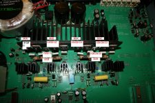
I have plugged in device, no inpuut/output connected, negative to chassis and postive on transistors and I noted results on output transistors. I have not done the other transistors below it however, the driver transistors?
I have plugged in device, no inpuut/output connected, negative to chassis and postive on transistors and I noted results on output transistors. I have not done the other transistors below it however, the driver transistors?
Attachments
- Status
- Not open for further replies.
- Home
- Amplifiers
- Solid State
- Rotel RA-940BX distorted sound