Hi everybody
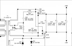
Can somebody point out what are the CR5 + CR6 (TC7+TC8) in Rockford Fosgate T10001bd component as they are missing in mine ?
How there are +- 58volts rails when the minus is connected to one end of the cap and the plus to the other. I don't get that, There is no ground ?
Schematics attached.
Can somebody point out what are the CR5 + CR6 (TC7+TC8) in Rockford Fosgate T10001bd component as they are missing in mine ?
How there are +- 58volts rails when the minus is connected to one end of the cap and the plus to the other. I don't get that, There is no ground ?
Schematics attached.
Attachments
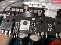
MUR1620CT and MUR1620CTR
Both have a G suffix for the newer, lead free parts.
Rockford BD amps have floating rails.
Both have a G suffix for the newer, lead free parts.
Rockford BD amps have floating rails.
Perry, big thanks
I've read your file "Class BD amplifier Theory and Operation" but still how to measure properly both rails + and - ?
Now if I reference the black probe to GND, i'm measuring only something like -65v, but I can't find any positive + rails anywhere. That's why I'm having doubts in the one of the rectifiers.
Amp actually powers up, but does not produce top half of the sinewave, the positive one. It came in without one of the irfp3415.
I could not find any shorted transistors, diodes or voltage regulators. Nothing visible. I've measured most of the resistors (not all of them) and they are in 1~2% tolerance range. Nothing is heating up abnormally.
I do have the auxiliary +-6v, +-10v, +-20v, but the +-16v are +-14.2v, not exactly 16v. Changed LM317 (U7) + LM337 (U8) аnd changed the resistors in the circuit, still the same +-14.2v. I don't know if something is dragging the voltage down equally to +- or this is supposed to be like this.
There is also something else that bothers me. On one of the MEHSA board there is J3 jumper, where two of the leads are connected to a unreadable resistor, reads 10.2 kilo-ohms. Is this the right value ? Can test the amp with the mosfets in place but without this jumper and resistor connection (without inserting the MEHSA BOARD back in the mainboard) ?
Attachments
You measure the rail voltage by measuring across the center legs of the positive and negative rectifiers.
The resistor on the MEHSA insulator is a thermistor. All of the thermistors should read approximately 10k ohms at room temperature. I don't know what you mean by unreadable.
What's the PC# on your board?
Using the calculator under item 25 on the audio troubleshooting page, entering the exact values from your amp and regulators, you can find the expected output voltage.
No any voltage on the center leg of the u1620r diode.
I don't know what you mean by unreadable - there was no marking on it. So this seems fine.
What's the PC# on your board? - will post once I get back home from work.
I've some issue with the flash content.
I don't know what you mean by unreadable - there was no marking on it. So this seems fine.
What's the PC# on your board? - will post once I get back home from work.
I've some issue with the flash content.
Are you using Safari?
Did you install the _371 Flash players?
Are any of the Flash files working?
Unmarked. I thought you meant unreadable, in some way, with your meter.
Not referenced to ground. You have one probe on one center leg and the other probe on the other center leg.
Did you install the _371 Flash players?
Are any of the Flash files working?
Unmarked. I thought you meant unreadable, in some way, with your meter.
Not referenced to ground. You have one probe on one center leg and the other probe on the other center leg.
Not referenced to ground. You have one probe on one center leg and the other probe on the other center leg.
So measuring the proper way +58,5v of rail voltage.
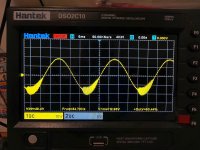
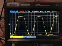
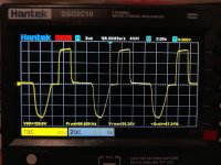
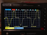
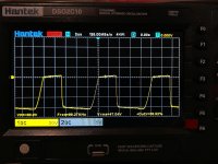
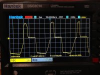
I've fitted some new irfp3415 but same thing as with the original ones. If I apply even a small loud at the speaker terminals the top half of the sinewave is not being produced.
Without a load there is a noisy sinewave at the lowest gain point, but if I increase the gain even a bit, same thing happens, the top half of the sinewave is cut off.
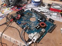
You can see in the attached images.
What i've noticed, if the amp stays idle for more than 1-2 minutes, q201, q202, u202, u204 and the output mosfets are getting hot. Current draw stays the same all the time at 2.4A.
Attachments
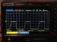
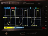
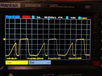
How far is the square wave shifting, above and below ground, on the rail switching FET (on the left of the amp)?
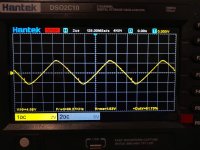
What's the amplitude (above and below ground) of the triangle wave on the integrator output?
What's the amplitude (above and below ground) of the triangle wave on the integrator output?
I will try to give as much info as a I can. Pictures are taken with no signal thru RCA jacks.
Section A runs much much cooler than B.
This is the A side
Section A runs much much cooler than B.
This is the A side
Attachments
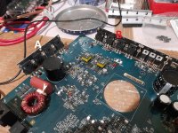
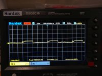

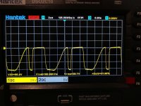
This is section B:
Attachments


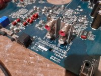
Are the current shunt resistors R290-292 reading, basically, a dead short across them?
Is the voltage on pin 8 of the audio driver ICs at a steady 10v?
What's the DC voltage on pin 3. Is it steady?
Is the voltage on pin 8 of the audio driver ICs at a steady 10v?
What's the DC voltage on pin 3. Is it steady?
Are the current shunt resistors R290-292 reading, basically, a dead short across them?
Is the voltage on pin 8 of the audio driver ICs at a steady 10v?
What's the DC voltage on pin 3. Is it steady?
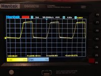
1. Yes, dead short
2. Do You mean U202 and U204 ?! Pin 8 is exactly 10.5v steady.
3. Pin is exactly 5v, steady too.
When you load the amp and get the distortion, do you get a similar change in the input or output of the audio driver ICs?
- Home
- General Interest
- Car Audio
- Rockford Fosgate T10001bd component identification