Hello,
Would like some help. Have been designing an amp using Bob Cordells book and have finally got somewhere after many hours. It is a double EF output with darlington VAS and darlington Vbe multilier. It passes the phase and gain margin tests in Bob's book.
Have been doing some THD simulation and get the following results.
All tests have been into a 4 ohm load at +/- 20V output.
1Khz sine wave = 0.02%
10Khz sine wave = 0.8%
20Khz sine wave = 0.8%
Unloaded 1Khz sine wave = 0.0001%
I'm thinking I may have a slew rate issue.
Are these anywhere near respectable?
The only thing is that the the odd harmonics dominate.
Paul
Something must be wrong there! Your THD numbers divided by 100 are normal numbers for SS amplifiers.
Greetz
Greetz
if youre using ltspice dont forget
.options plotwinsize=0
.options noopiter
or the compression will cause artificially high THD
.options plotwinsize=0
.options noopiter
or the compression will cause artificially high THD
Turned the compression off and increased the resolution of the simulation and now have the following.
0.0095% @ 20Khz +/-20V output into 2 ohms.
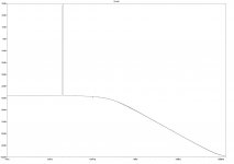
Done some square wave simulations no overshoot or ringing but the slew rate looks very slow. What is a good slew rate to aim for? Or am I missing something in LTspice?
0.0095% @ 20Khz +/-20V output into 2 ohms.
Done some square wave simulations no overshoot or ringing but the slew rate looks very slow. What is a good slew rate to aim for? Or am I missing something in LTspice?
one reasonable estimate of the required slew rate would be that which would allow a 20 kHz full power sine wave without strain. Assume 20 volt peaks, based on your +/-20 Volt rails, and that gives you 20,000*20*2*pi=2.5 Volts/us.
Now, that would leave no margin...e.g. the amp would be at the edge of slew rate limiting, which isn't good...so...how much safety margin? 4x would say 10 v/us, 10x would say 25 v/us.
Perhaps a reasonable to extreme test would be to use an intermod test...drive the amp to a bit below full power output with a 20 kHz sine wave, and use some of the rest of the swing with a simultaneous 1 kHz sine wave, then look for the intermod sum and difference products in the FFT.
Update My Dynaco
Akitika GT-101 Audio Power Amplifier Kit
Please go easy on this...
djoffe, sound reasonable. Just trying to understand the test you suggested.
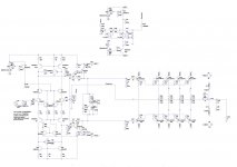
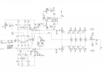
Elvee, here is the schematic, and a couple of figures...
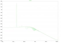
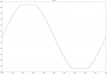
There is some overshoot on the square wave. These appeared after removing the ideal current source.
The square wave is offset. After a number of cycles it centres itself. Is this slew rate again?
Please bear in mind this is my first attempt at designing an amp. Have been using the late Professor Leaches site and Bob Cordell's book only. Not trying to do anything ground breaking or flash. Just aiming for a solid design.
Thank you for the help. 🙂
djoffe, sound reasonable. Just trying to understand the test you suggested.
Elvee, here is the schematic, and a couple of figures...
There is some overshoot on the square wave. These appeared after removing the ideal current source.
The square wave is offset. After a number of cycles it centres itself. Is this slew rate again?
Please bear in mind this is my first attempt at designing an amp. Have been using the late Professor Leaches site and Bob Cordell's book only. Not trying to do anything ground breaking or flash. Just aiming for a solid design.
Thank you for the help. 🙂
Attachments
Last edited:
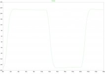
It looks like you have plenty of slew rate...It's hard to tell but it looks to be between 20 and 40 v/us.
The intermod test works like this. A high slew rate signal tends to max out the first stage current, pushing all the tail current into one or the other input transistor. If it does that to the extreme, it changes the gain of the amp, that even with feedback present, shows up as intermod distortion.
Given the slew rate that you showed, I don't think you'll have a problem.
I will say, that the schematic image was a bit hard to see.
Akitika GT-101 Audio Power Amplifier Kit
Update My Dynaco
That's a minor issue. It could be eliminated by fine-tuning a small cap across the main FB resistorThere is some overshoot on the square wave. These appeared after removing the ideal current source.
No, that is caused by your servo running for ever in the pre-sim period with the square wave high or low.The square wave is offset. After a number of cycles it centres itself. Is this slew rate again?
Simplest fix is to disable the servo for this kind of test, it has little influence anyway.
At first sight, the SR is something like 20V/µs. Not huge, but sufficient.
If you want to improve it you have to determine through which capacitances the current flows during the transitions.
You can then try to reduce the capacitances in question, or increase their charging currents.
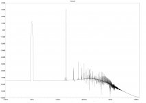
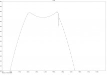
Intermodulation fft and hopefully larger schematic
Thank you for your replies. 🙂
Have tried to make schematic easier to read. These are the first images I've posted on this forum so need to learn.
djoffe, have tried to implement your suggested test and have attached the fft produced. Not sure how to interpret though.
Elvee, have tried disabling the servo and the result was as you said would happen. Going to try and improve slew rate by looking at the capacitor currents. "Gut feel" tells me stability may be affected by this though.
One thing I have noticed is that it clips very hard and sticks badly. Think maybe adding baker clamps would be a good idea.
Paul
Attachments
There are no free lunches.. etc.."Gut feel" tells me stability may be affected by this though.
Thank you for your replies. 🙂
djoffe, have tried to implement your suggested test and have attached the fft produced. Not sure how to interpret though.
Paul
The 19 kHz sidebands (spikes near the 19 kHz) are 100 dB down...you have enough slew rate for any forseeable audio signals.
No free lunches. Just been trying to increase the slew rate and all I get is a reduction in stability and no increase in slew rate.
Thank you, djoffe, good to know as I can't find the limiting factor regarding slew rate (yet).
My latest little play has been implementing basic baker clamps. There is still sticking at the rails. The dip after sticking is about 3v. Both halves of the sine wave are identical.
More research and experimentation required. 😀
Attachments
Sticking certainly has more objective impact (if you use your amps at their limit) than pushing the slew rate beyond 20V/µs.
It is more of an intellectual satisfaction. Which doesn't mean it isn't worth pursuing. When all the rest is fixed.
It is more of an intellectual satisfaction. Which doesn't mean it isn't worth pursuing. When all the rest is fixed.
Looks like I'm learning about LTspice as much as I am about amplifiers. Specified the rise and fall times of the pulse and now I measure 104V/uS slew rate. A bit more respectable.
Are R23-C9 drawn as intended? Perhaps their purpose is to introduce an LPF with corner frequency around 8 MHz, to reduce RF interference?
I also wonder whether it may be a false economy to omit emitter resistors from Q31, Q32? If their VBE mismatch is ± 5 millivolts, is the resulting bias current acceptable to you?
Finally, isn't it more common to specify 3A or even 5A parts for catch diodes D11 and D12?
I also wonder whether it may be a false economy to omit emitter resistors from Q31, Q32? If their VBE mismatch is ± 5 millivolts, is the resulting bias current acceptable to you?
Finally, isn't it more common to specify 3A or even 5A parts for catch diodes D11 and D12?
It looks hellish complicated for such a modest goal. The very thought of soldering so many components offends my innate sense of laziness.😀Not trying to do anything ground breaking or flash. Just aiming for a solid design.
BTW, shouldn't the top of C2 and the bottom of C3 be connected to the positive supply and the negative supply rail respectively instead of ground? That should help the PSRR a bit. (These are the capacitors near the inputs of the two halves of the VAS).
Maybe related to the fact that there's no current limiting (that I can see) for Q8 and Q9 in the VAS. Simplest solution is to add resistors in series with their collectors.There is still sticking at the rails.
Update on development
Update time... 🙂
Have taken note of the suggestions. Tried each to see the effectiveness.
Have made the following changes:
- The clipping problem was solved using feedback baker clamps as
detailed on Bob's book.
- Changed the design to a triple and changed the VAS and Pre driver
transistors.
- Increased the gain slightly.
- Added emitter degeneration to the current source.
- Changed amp input network.
This has brought the thd figure for near full power @ 20Khz into 2 ohms down to 0.005%. Still appears to have adequate phase and gain margins. The slew rate has increased to 120v/uS.
Should I implement some sort of current limiting? May do this at the power supply though.
What do you guys think?
Am I mad??? 😀
Godfrey - It's not the soldering that worries me its the pcb layout. And whether I can get it to work in reality.
Cheers
Paul
Attachments

- Status
- Not open for further replies.
- Home
- Amplifiers
- Solid State
- Respectable THD levels for double EF Amp