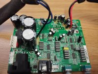
I have a Focal Alpha 80 monitor that kept blowing fuses. It looks like the culprit was a TDA7294 on the LF channel that exploded spectacularly. Presuming this was just someone putting too much gain for the amp IC to handle, I replaced it and the fuse. On turning it on without any output, the power LED sputtered for a moment and there was a distinct pop. I turned it off before the fuse blew again and had a look inside. The second TDA7294 had exploded even more spectacularly leaving a dumpster fire's worth of smoke in the unit.
I removed it and looked for other issues but could not find any. The transformer is outputting 28V AC and 16V AC (slightly more than the rated 25V and 14V but I can't see that that is an issue). Pins 7/13 are measuring 39V and 8/15 are -39V. Cutting it fine with the rated voltage of 40V for a TDA7294 but again, should work fine. The equivalent pins on the HF channel are +/- 20V. There are no apparent visual problems but I may be missing something -- if anyone suggests measurements worth taking, I would be happy to try them.
Was the first blown amp due to too much gain, and did I just get unlucky with my replacement TDA7294? Admittedly I got a no-name part off AliExpress as virtually no money is coming out of this repair, but I'm wondering if that was a false economy. I have now ordered one from ST but that will take a little time to get here. Any pointers appreciated.
Oh, and I'm ashamed of the state of the pins where the 7294 goes, but two explosions had pretty much destroyed any chance I had of desoldering it cleanly 🙃
Attachments
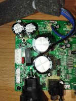
For one thing, some of your solder pads on both sides are damaged and need repair. That was likely do to rough removal of the IC.
I'd check the small caps around the IC. The TDA7294 is VERY sensitive to overvoltage on pins 7 and 8 in relation to pins 13 and 15 (see example circuit diagram below). Even if operating under the max voltage, the chip can't have more voltage on 7 and 8 at any given time than on pins 13 and 15.
It only takes a split second transient when the smaller filter caps around the IC are charging or discharging (or one of them is bad). Under no circumstances should pins 7 and 8 have more voltage than pins 13 and 15, even for a fraction of a millisecond ie. when the power is turned on/off and the caps are charging or dis-charging unevenly in relation to each other.
So my advice would be to remove and test all the small electrolytic caps around the IC. The solder pads need repairing as well. If those aren't reliable, you'll be wasting alot of ICs and further damage the PCB from excessive component swapping. You may want to invest in a cheap desildering tool that sucks the solder off the pads instead of desoldering wick. I always re-flow the old lead free solder first with 60/40 lead/tin solder before removing the IC. This helps with removal of the old solder.
There's also the obvious issue of counterfeit parts. Be sure to buy your ICs from a reputable source.
Last edited:

AFAIK it can have to do with revision of the chip and also I recall an issue with either the mute or the standby pin causing it (in certain revisions/years of production). It is for sure a known failure.
Thank you both for the replies. I removed the five electrolytic caps around the IC, and unfortunately all are reading within a few % of their ratings. I'm aware the solder pads look very suspect, and I intend to repair them before putting this back into action, but for now all are measuring perfect continuity with their intended connections, both before and after soldering on the last TDA7294. The worst-hit solder pads are unconnected on that side.
On a desoldering tool, I have bought so many trinkets over the last year that my wife will kill me if yet another box comes through the door! It would be nice to use the tools I have now. The reflowing with 60/40 lead solder was a great shout though -- it made taking the caps off a much cleaner job, so thank you.
(Also, I tried to recreate the test circuit on a breadboard but I lack enough leads to have both V+ and V-. I wanted to stress-test these AliExpress ICs to see if voltages near 40V are an issue but that project might have to wait...)
Do you know in what way the mute/standby pins caused this issue? The previous posts I read were a bit unclear on this. I'm not really sure how mute/standby pins really work on a circuit level.
Another way would be to cut all legs on the defective IC.
Then use your soldering iron to heat up the pads one by one while carefully removing the pins.
Removing 15 "unsoldered" pins in one go on through plated PCB´s is much harder.
Then use your soldering iron to heat up the pads one by one while carefully removing the pins.
Removing 15 "unsoldered" pins in one go on through plated PCB´s is much harder.
Sorry, I just replaced many of them (in Linn amplifiers) and only much later read the reasons for failure. My mind just says “avoid TDA7293/7294”.
They're cheap amp ICs capable of decent performance. The problem is usually safe area operating parameters not being exceeded or approached. The LM3886 and LM3875 IMO sound better and are more durable than the TDA7294.
I have a few questions and remarks here.
First off, I find it incredible, irritating and insulting to post a question here about an electronic circuit problem, and not even posting a schematic, but only a picture of a PCB.
We, electronic engineers can't do anything without a schematic. Posting a picture of a PCB is posting a picture of a food dish and ask why it does not taste well, without providing the recipe.
Then, as @profiguy says, there is the risk that the voltage on pin 7/8 is more than pin 13/15 which could destroy the IC. While I can totally imagine that circuits cannot tolerate that (for example if a forward bias would result and unlimited current could flow) I don't see this warning in the datasheet.
On the contrary, in the datasheet a "high efficiency" circuit is proposed. With pin 7 tied to +40VDC and pin 13 to +20VDC. Where the voltage on pin 13 can be increased to +40VDC apparently at higher output level. But this very clearly allows a much higher voltage on pin 7 than on pin 13. Same goes for the negative side. On the contrary, the datasheet explicitly states that 4 separate power pins are provided to split the power supply between signal and power stage.
So coming back to my first statement, what is the circuit diagram? Standard application or high efficiency? And what is the substantiation that pin 7 is not allowed to carry a higher voltage than pin 13?

Finally, the datasheet states that the absolute max power supply voltage is +/- 100VDC, without signal. And +/-40VDC with signal. So I find a supply voltage +/-39V a fairly thin on max specification. Even more because we don't know how the output is connected during power-on, and more so what happens at the input. Is there a risk for a transient during switch on which could overload the output stage?
First off, I find it incredible, irritating and insulting to post a question here about an electronic circuit problem, and not even posting a schematic, but only a picture of a PCB.
We, electronic engineers can't do anything without a schematic. Posting a picture of a PCB is posting a picture of a food dish and ask why it does not taste well, without providing the recipe.
Then, as @profiguy says, there is the risk that the voltage on pin 7/8 is more than pin 13/15 which could destroy the IC. While I can totally imagine that circuits cannot tolerate that (for example if a forward bias would result and unlimited current could flow) I don't see this warning in the datasheet.
On the contrary, in the datasheet a "high efficiency" circuit is proposed. With pin 7 tied to +40VDC and pin 13 to +20VDC. Where the voltage on pin 13 can be increased to +40VDC apparently at higher output level. But this very clearly allows a much higher voltage on pin 7 than on pin 13. Same goes for the negative side. On the contrary, the datasheet explicitly states that 4 separate power pins are provided to split the power supply between signal and power stage.
So coming back to my first statement, what is the circuit diagram? Standard application or high efficiency? And what is the substantiation that pin 7 is not allowed to carry a higher voltage than pin 13?
Finally, the datasheet states that the absolute max power supply voltage is +/- 100VDC, without signal. And +/-40VDC with signal. So I find a supply voltage +/-39V a fairly thin on max specification. Even more because we don't know how the output is connected during power-on, and more so what happens at the input. Is there a risk for a transient during switch on which could overload the output stage?
- Home
- Amplifiers
- Chip Amps
- Repeatedly blown TDA7294 on a Focal Alpha 80 monitor