I designed this boost converter with a UC3843 chip using all SMD parts. I based the current limiting section around the design found on this page, although i honestly don't totally understand it. http://dion.swamp.dk/carpower.html
If anyone is intersted, i would love to hear any input/suggestions about my design/if it will work.
Thanks, Chris
If anyone is intersted, i would love to hear any input/suggestions about my design/if it will work.
Thanks, Chris
Attachments
Actually, i redesigned it, built it and it works great. Im getting something like 90% efficiency for 13.8v in and 19.5v out
Just a thought:
I would minimize the parasitic capacitance on MOSFET's drain (also applicable for diodes) by reducing the copper area. In this way the EMC behavior can be improved.
I know that reducing copper area is contradictory if you think for power losses but the generated heat is spreading pretty well through PCB itself.
Moreover, a massive groun plane will play a significant role for both EMC and cooling.
cjk2-
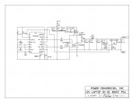
Do you have a schematic? It's probably a variation of the many out there as this topology can't vary too much. Here is a 2-F DC-DC I did for one of my ham radio buddies a couple of years ago. It uses an SG3525 alternately switching two MTP75N06s at about 100kHz (50kHz per MOSFET). The basic topology is much like your '3843-driven one, except that both inductors are wound on the same toroid, bifilar. Output diode is MBR2545CT, putting out 19.5V at over 8A, when necessary. Whole thing gets only moderately warm.
Do you have a schematic? It's probably a variation of the many out there as this topology can't vary too much. Here is a 2-F DC-DC I did for one of my ham radio buddies a couple of years ago. It uses an SG3525 alternately switching two MTP75N06s at about 100kHz (50kHz per MOSFET). The basic topology is much like your '3843-driven one, except that both inductors are wound on the same toroid, bifilar. Output diode is MBR2545CT, putting out 19.5V at over 8A, when necessary. Whole thing gets only moderately warm.
Attachments
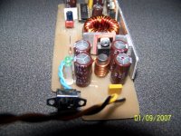
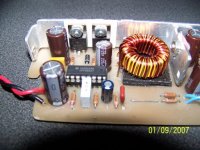
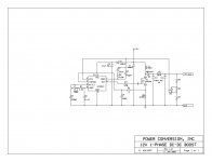
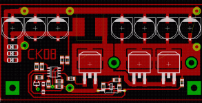
Sadly I never drew a schematic for it, I usually just do it in my head. My design is based on this one though. The current limiting system is all that I don't totally understand, and it seems to work well enough based on the prototype I built. Anyway, I have attached a full eagle PCB file for anyone interested. I went with a to-220 MOSFET and diode for better cooling. I intend to have a few of these boards professionally made soon.
Attachments
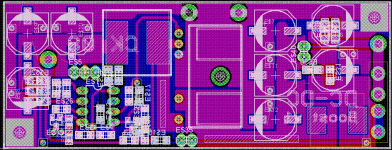
I must say... That board looks professionally done! BTW, Bob Blick's circuit is not a boost ckt, but rather a Single-Ended Primary Inductance Converter or SEPIC circuit, where the input voltage can be either above or below the output. The two inductors act to either boost or buck the incoming voltage. If coupled together, as illustrated in Mr. Blick's schematic, the circuit becomes a bit more efficient.
- Status
- Not open for further replies.
- Home
- Amplifiers
- Power Supplies
- Rate my 12v to 19v converter please!