Re: v7: added resistors
That's interesting, could you elaborate this issue and your experience?
I am using a resistor in similar place, but rather in 22R-47R range, how did you determine 1k?
regards
Adam
tcpip said:Also added a resistor (R40) at the input, because without it, and with C2, there is a likelihood of oscillation (Q1 can become a common-base oscillator if its base finds an AC ground path, and C2 will provide that path if I don't add R40).
That's interesting, could you elaborate this issue and your experience?
I am using a resistor in similar place, but rather in 22R-47R range, how did you determine 1k?
regards
Adam
Re: Re: v7: added resistors
I will decide the value later. The idea is that you use as high a resistor value here as you can, to damp any oscillations as fast as possible. But you can't go infinitely high, because it'll affect the DC offset and so on, so you limit it to something you can get away with. With an input impedance resistor of 10K, I thought I could certainly get away with one-tenth that for this one.
Rod Elliott too takes this care in the P3A. He too uses one-tenth of his input impedance resistor for his base resistor.
Really sorry to disappoint you, but I don't have any experience in building this amp. I've just put in the places for this resistor in the schematic and PCB layout, so I don't know what value is correct. The only background I have about this resistor is the discussion I've had with a veteran amp-building friend who had faced problems with oscillations and figured out that this AC ground path is the cause.darkfenriz said:That's interesting, could you elaborate this issue and your experience?
I am using a resistor in similar place, but rather in 22R-47R range, how did you determine 1k?
I will decide the value later. The idea is that you use as high a resistor value here as you can, to damp any oscillations as fast as possible. But you can't go infinitely high, because it'll affect the DC offset and so on, so you limit it to something you can get away with. With an input impedance resistor of 10K, I thought I could certainly get away with one-tenth that for this one.
Rod Elliott too takes this care in the P3A. He too uses one-tenth of his input impedance resistor for his base resistor.
TCPIP,
I'm curious about your power resistor layout? How did you plan on mounting those? They seem to all be overlapping on your latest PCB layout.
As someone else mentioned earlier, have you considered standing them up on end? It would free up a LOT of space on the board, and look nice and neat as well.
..Todd
Hi Todd,
I can shift R34 back to vertical, but at least R35 and R37 are best done horizontally, so that they can reach from the far OPS devices to the centre. If I mount those vertically, it's hard to draw wide tracks from them to the central block.
I'm thinking of mounting R35, R36, and R37 on the top surface of the board, raised about a quarter inch to allow the smaller resistors to lie below them. I'm thinking of mounting the slanted one (R34) below the board. I've seen other small amp PCBs where resistors (and other components) are mounted that way. I'm not saying this is the best but then if I had the chance to make a PCB twice this size, I'd probably do many things differently, retain the OPS protection circuits, and try to aim for a single-layer PCB to begin with. 🙂taj said:I'm curious about your power resistor layout? How did you plan on mounting those? They seem to all be overlapping on your latest PCB layout.
I'm all for vertical resistors but power resistors are heavy, and standing them vertically may not make them very mechanically strong. I don't want the solder joiints to crack if someone shakes the amp. I had put R34 vertically earlier, but it was too close to the inductor L1 and might not have given enough space for me to put the inductor, so I was thinking of fitting R34 vertically below the PCB. Later I thought that if I do fit it below, why not horizontally?As someone else mentioned earlier, have you considered standing them up on end?
I can shift R34 back to vertical, but at least R35 and R37 are best done horizontally, so that they can reach from the far OPS devices to the centre. If I mount those vertically, it's hard to draw wide tracks from them to the central block.
separated the CCS
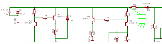
Have created a separate CCS for the VAS (I think!). Will you please check it? See Q18 and R41.
What value should I set R41 to? I guess it can be anything which allows about 2-5mA to flow from supply rail to ground, right?
Can I knock off R42 now?
Have created a separate CCS for the VAS (I think!). Will you please check it? See Q18 and R41.
An externally hosted image should be here but it was not working when we last tested it.
What value should I set R41 to? I guess it can be anything which allows about 2-5mA to flow from supply rail to ground, right?
Can I knock off R42 now?
Hi,
R41 should allow about half the current that the CCS passes, but as you suspected there is a very wide accepatable range. You may find that one small range of current particularly suits Speed OR Stability OR temperature compensation. If you are VERY lucky you may find that you can get two of these, but I have neither the patience nor the expertise to recognise the desirable characteristics (I may have omitted something even more important).
R7 and R42 can be omitted.
The CCS on the LTP can operate from a much reduced Vrail so a resistor and cap could usefully take up the space you gained. ie. r9 is deleted and a new resistor is inserted between C5 and Q4.
So there is a possibility that the value of R41 will affect stability? I'm beginning to feel a bit nervous.AndrewT said:R41 should allow about half the current that the CCS passes, but as you suspected there is a very wide accepatable range. You may find that one small range of current particularly suits Speed OR Stability OR temperature compensation.
Incidentally, if I have to take your feedback and that of others on the other thread I started (about Fig 11.4 Blameless), I'll be running VAS really hot, at perhaps 25mA. In that case, R41 will have to carry about 10mA of current? The current setting is for about 2-3mA.
Cool. I had hoped as much.R7 and R42 can be omitted.
Great.The CCS on the LTP can operate from a much reduced Vrail so a resistor and cap could usefully take up the space you gained. ie. r9 is deleted and a new resistor is inserted between C5 and Q4.
BTW, won't I need a resistor between C5 and Q8, not Q4? If I don't put the resistor to the right of C5, it won't be a smoothing voltage divider, I thought. If it's just to reduce rail voltage but not to smooth it, what benefit does it give?
hi tcpip!
Why don't you place C4&C13 between input stage and VAS ?
I'm using a Symmetrical amp and use RC filter for suplly rail. If I place those cap like your way, my amp ocssilated
Why don't you place C4&C13 between input stage and VAS ?
I'm using a Symmetrical amp and use RC filter for suplly rail. If I place those cap like your way, my amp ocssilated
Hi Tc,
R38/C5 reduce rail ripple AND keep Vrail high. Q8 needs to swing rail to rail to allow the output stage to work to maximum output. C5 will probably benefit from being increased. (R9=0.0)
Rextra(between C5 and Q4)/C3 reduce rail voltage to some lower value (anywhere between 50% and 90% of Vrail) and feed the tail of the LTP CCS with an almost completely ripple free supply.
You mean C14 and C3?thanh said:Why don't you place C4&C13 between input stage and VAS?
In that case, will it be better if I just allow for separate regulated 15-0-15V supply (of the kind used for opamps) for just the input stage?AndrewT said:R38/C5 reduce rail ripple AND keep Vrail high. Q8 needs to swing rail to rail to allow the output stage to work to maximum output. C5 will probably benefit from being increased. (R9=0.0)
Rextra(between C5 and Q4)/C3 reduce rail voltage to some lower value (anywhere between 50% and 90% of Vrail) and feed the tail of the LTP CCS with an almost completely ripple free supply.
NO!.
the LTP needs full voltage on the collector load.
It's just the tail that can operate with less rail voltage.
With resistor load for the tail current you want a very high rail voltage to try to achieve constant current.
With a CCS loading the tail, then there is not such a need for a high rail voltage and you can take advantage of this by using a long time constant RC to attenuate any ripple on the tail, or cascade two RCs, or add a zener instead of the second cap. Many options due to using the CCS.
This paragraph decribed my thought wrongly. I'm sorry!hi tcpip!
Why don't you place C4&C13 between input stage and VAS ?
I'm using a Symmetrical amp and use RC filter for suplly rail. If I place those cap like your way, my amp ocssilated
Yes!quote:
Originally posted by thanh
Why don't you place C4&C13 between input stage and VAS?
You mean C14 and C3?
You can see my schematic
amp form thread "Help me! nice amp but noisy"
Look post#51 by AndrewT
Perhaps I decribed the sound effect which AndrewT mentioned 🙂If you do add a resistor (to listen for it's sound effect)
So, did you finally manage to lick the noise problem with your amp and sound card?thanh said:You can see my schematic
amp form thread "Help me! nice amp but noisy"
Does "lick" mean "beat" or "overcome"? If it is like that, my answer is no.So, did you finally manage to lick the noise problem with your amp and sound card?
My amp is sometimes noisy , and sometime is not with this filter.
I thought that capacitor can cause noise so I tried to place cap like you way---> occsilate, noise 😉
Do you know why I add resistor for rail supply ? I hoped that it can beat noise but It seem to be useless. If it has a effect, it is difficult to recognize the change
You can also taste this favor. Ypu add a resistor and place cap like your way
This is a experience which I want to share you
Bye!
Yup.thanh said:Does "lick" mean "beat" or "overcome"?
Let's see how my experience works out. 🙂You can also taste this favor. Ypu add a resistor and place cap like your way
This is a experience which I want to share you
Going by the intermittent nature of your problem, are you sure it's not due to a dry solder or a faulty component? Have you built a second unit and is the behaviour identical to the first? Have you tried keeping the amp PCB far away from power supply components? Have you tried driving the amp from something other than a PC sound card (e.g. a DVD player's audio output)? Just trying to suggest what I'd try, given my very limited knowledge. 🙂
v10: with separate CCS for input and VAS
I separated the CCS of the input stage from that of the VAS, and made the VAS CCS into a double-transistor CCS of the kind Randy uses in all non-mirror-image schematics. (Apparently they regulate current better than double-diode or LED-based CCS, and also give better PSRR, which is important for single-ended topologies.)
The PCB layout has been updated to accept the second CCS (Q18 and passives) and all tracks running to INGND or the PGND points have been separated, i.e. unrelated sections of the circuit do not share a common track to one of the ground points. So each ground point now looks like a local star-ground.
Awaiting any further feedback.
I separated the CCS of the input stage from that of the VAS, and made the VAS CCS into a double-transistor CCS of the kind Randy uses in all non-mirror-image schematics. (Apparently they regulate current better than double-diode or LED-based CCS, and also give better PSRR, which is important for single-ended topologies.)
An externally hosted image should be here but it was not working when we last tested it.
The PCB layout has been updated to accept the second CCS (Q18 and passives) and all tracks running to INGND or the PGND points have been separated, i.e. unrelated sections of the circuit do not share a common track to one of the ground points. So each ground point now looks like a local star-ground.
An externally hosted image should be here but it was not working when we last tested it.
Awaiting any further feedback.
Yup... I know what you mean. Let me see if I get other feedback... I'll make all the changes together.thanh said:This is my opinion. VAS must be front of a RC filter
- Status
- Not open for further replies.
- Home
- Amplifiers
- Solid State
- Randy Slone "Fig 11.6" amp, modded: will work?