Also, you have corrected the values of the resistors in the Vbe multiplier. In the original schematic, they were too low. You have to remember that the Vbe transistor is actually a current source in a feedback loop, so if these resistors are of low value (but the ratio is correct), most of the current will pass through them, and not through the Vbe transistor, reducing the Vbe transistor's influence on the bias voltage. This is actually sometimes used to trim the Vbe multiplier when it overcompensates, but in your original schematic, the resistors were much too low.
ilimzn said:Also, you have corrected the values of the resistors in the Vbe multiplier. In the original schematic, they were too low. You have to remember that the Vbe transistor is actually a current source in a feedback loop, so if these resistors are of low value (but the ratio is correct), most of the current will pass through them, and not through the Vbe transistor, reducing the Vbe transistor's influence on the bias voltage. This is actually sometimes used to trim the Vbe multiplier when it overcompensates, but in your original schematic, the resistors were much too low.
Hi,
I try to get the resistor ladder current to be about ten times the Vbe multiplier base current.
Usually 0.5mA to 1mA in the resistors gets me to a range of 5mA to 15mA of quiescent Vbe current.
Are you saying this range of resistor currents is too high or is it acceptable?
How high does the resistor current have to become to effect a reduction in the temperature compensation? A current ratio resistor/Vbe recommendation would do here.
Xitronics,
What is happening right now is you have far too much loop gain and the roll off slope at the 0dB cross over point is >>20db per decade. To address your oscillation problem the loop gain needs to be reduced.
Insert a cap of between 100pf to 1nF between pin 6 if the op amp and pin 2. Use the lowest value you can get away with. This should tame it
Good luck.
Bonsai said:Xitronics,
What is happening right now is you have far too much loop gain
Hi,
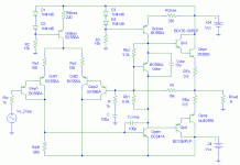
The excessive loop gain offered by opamp is a problem here. So I have replaced it with a differential pair followed by CE stage. Its also bcoz there are very few low-cost high-voltage opamps available. Please have a look at the new design attached.
Here oscillations is the only potential problem coz the open loop gain is still very high. Please comment on it.
and the roll off slope at the 0dB cross over point is >>20db per decade.
didnt follow.. could u simplify it.
________
Prasanna
Attachments
Hi,
start by removing the darlingtons around the input pair.
Then try adding an emitter resistor to the VAS.
Then try balancing the currents through the two halves of the input LTP.
start by removing the darlingtons around the input pair.
Then try adding an emitter resistor to the VAS.
Then try balancing the currents through the two halves of the input LTP.
You have accidently connected rb1 to the feedbacknode!
Also, connect the 2 emitters of the drivers with a resistor (maybe 150ohm) to bias them. Otherwise you will have ugly crossover distortion.
Mike
Also, connect the 2 emitters of the drivers with a resistor (maybe 150ohm) to bias them. Otherwise you will have ugly crossover distortion.
Mike
Adding emitter resistors to drivers has indeed made the output free from any crossover problems. Darlington pair at diff amp stage is removed as suggested.I am also thinking of increasing Re of the diff transistors to reduce TIM. 100 pf feedback capacitor is forming the only dominant pole in the circuit at 2Khz and so there is and no sign of oscillations. Gain crossover is at 2Mhz. Slew at 7V/uS - just about sufficient.
I dont find a proper circuit to auto-balance the diff amp currents under static conditions. Okay it can use a pot to with Rc or its current source's Re to do so but the setting will only survive for a short duration as the thermal variations in the two transistors and also the other parasitic variations will cause the balance to be broken.
Please comment.
___________
Prasanna
- Status
- Not open for further replies.
- Home
- Amplifiers
- Solid State
- Quiescent Current Control in Class AB..?