Hello all,
I have been working for some time on my first DAC project (CS8420, SM5847 (if I can find one!), PCM1704), and am currently working on the PCB design. The PCB will be 2 layers, and am wondering what the proper method is for grounding the digital and analog sections; it seems the more I try to learn about this subject, the more different opinions I find, and the more confused I become...
I know that most mixed signal designs split the digital and analog ground planes to avoid noise from entering the analog section, connecting at only one point, often under the dac or adc chip. I have also read that the dac chip should be considered an analog part and should rest entirely on the analog ground plane.
An article I found on the Analog Devices web site:
http://www.planetee.com/planetee/servlet/DisplayDocument?ArticleID=593
suggests that the two ground planes should be "kept separate all the way back to a common system 'star' ground, generally located at the power supplies."
This is the same technique used by Erland Unruh in an article a couple years back in Audio Electronics magazine.
However, I have also been re-reading the article posted on Marc Heiligers DAC page:
http://members.chello.nl/~m.heijligers/DAChtml/dactop.htm
by Guido Tent, an EMC engineer at Philips who suggests NOT splitting the ground plane, but keeping it closed:
http://members.chello.nl/~m.heijligers/DAChtml/Supply_decoupling.pdf
He states that (with proper decoupling of all chips and the use of lossy ferrite beads on all power feeds) splitting the ground plane creates a huge loop which "leads to high emmision, and a higher chance of inter-system pollution."
I had also considered using isolators such as the Burr Brown ISO150's (as used by Parts Connection on the DAC3.1) to isolate separate digital and analog groundplanes. Would this help address the poblem, or would these devices just be another source for noise and jitter?
So what should I do? I am using lossy ferrites and SMD polymer electrolytics for local decoupling for each chip.
Any feedback, or links to articles on this subject would be greatly appreciated.
Thanks!
Mark
I'm afraid I don't have any answers for you, but I know exactly how you feel. The more research you do, the more confused you get, as lots of possible solutions and 'best techniques' seem to be conflicting and at complete odds with one another, and lead to impossible PCB layout problems.
In my last DAC, I eventually just bit the bullet and implemented a split groundplane, joined in the middle, with completely seperate power supplies (4 x 12v Sealed Lead Acid Batteries for the analog stage) and lots of ferrites and SMD decoupling caps and components. It sounded fine.
If I ever get around to building another DAC, I'll isolate the thing completly by using a transformer coupled digital input, ISO150's between the digital and DAC/Analog stage, and seperate isolated power supplies again. A bit more physical seperation between the two stages wouldn't go amiss either (Oh no, now you've got me thinking...)
I think the only way to be certain something works or doesn't work is to build a prototype, measure it and then modify and measure again, which is outside the abilities of most DIYers to do it accurately. We're not interested in obtaining international EMI certification, we only want to make sure it doesn't interfere with our music.
Cheers, Adrian
Digital Grounding
Here is a good place to start research. I highly recomend his book also. www.sigcon.com
H.H.
Here is a good place to start research. I highly recomend his book also. www.sigcon.com
H.H.
Follow Analog Devices advice. The subtle problem with a ground palne is that it can act like an antenna. You need to bypass all wires in/out of the device better.
Don't split the ground planes too far apart: it will cause a larger loop for the currents to circulate.
Can't get the NPC chip still? Let me know.
Jocko
Don't split the ground planes too far apart: it will cause a larger loop for the currents to circulate.
Can't get the NPC chip still? Let me know.
Jocko
Thanks for the feedback!
The sigcon site is great- most of it is way over my head, but I have already found some useful information.
I suppose I will go for the split ground plane like Adrian, bridging the two sections on the board. I'm thinking that using an entirely separate power supply for the analog section with separate power transformer might be a good idea, so that the only ground connection between analog and digital section would occour at the ground bridge on the board. Or would this be coutrerproductive? (I still want to think of digital signals like analog signals, although I know they behave quite differently) Could this Increase system noise? Should power supply grounds be tied together before they enter the board?
Or maybe the ISO150 isolators are the best solution. Anyone else have any experience with these?
Lastly, what kind of bypassing do you recommend Jocko? (and look for an email regarding that impossible to find 5847 chip)
Mark
If you place the receiver circuitry and maybe even the filter on the digital plane, include 100-300 R series resistors in the signal line and place all of the DAC on the analog plane, the separate plane approach might be OK. You will have some loss of noise margin on the digital signals if the two grounds are connected with too much inductance in between. This is probably not going to hurt signal transmission but may screw up the timing (jitter!) which is only critical if the clock is not generated in or right next to the DAC chip.
Do not by any means connect the digital ground and supply pins of the DAC to the digital network! Any noise between the two ground planes will end up inside the DAC substrate.
Eric
Do not by any means connect the digital ground and supply pins of the DAC to the digital network! Any noise between the two ground planes will end up inside the DAC substrate.
Eric
Have you looked at the price of those isolator thingies??? I suspect not. You are on the right track......keep going. Bypassing: 0.1 uF caps everywhere you can shove them, the big electrolytics don't seem to be that critical. I've built ones with nothing, and others with big caps everywhere. Personal preference works here.
Jocko
Jocko
I don't think the ISO150 is worth it. In fact,
it is probably worse than having a little noise
on the ground plane. You will need two
IS0150s for a stereo DAC: one for the clocks
and one for each data line. Unfortunately,
the worst-case interdevice time delay is
quite high, so you might wind up with more
time domain problems with your digital
signal than you would other wise have.
That is to say, your clocks and your data
might not arrive together.
Keep it simple: decouple each IC power pin
with a big cap and a fast cap, liberally
employ ferrite beads. You'll have as clean
power and ground planes as you can hope
for in a 2-layer PCB layout.
Stay away from the opto's. I got a board here with an opto coupled digi-analog split. Nothing but trouble concerning noise/hum. Both grounds are completely split, but what do you do with the cables/connectors going out? The timing problem with opto's can be solved by using a pll and VCXO on the analog side driving SH circuit. Only a single Fs then unless you switch VCXO's.
I would go with the single plane. Once your circuit is done, fill both sides with copper and lay via's where you can connecting both planes together. Make sure to bridge any important gap in the gnd-copper and try to have gnd under each Vcc trace.
Only 0.02
I would go with the single plane. Once your circuit is done, fill both sides with copper and lay via's where you can connecting both planes together. Make sure to bridge any important gap in the gnd-copper and try to have gnd under each Vcc trace.
Only 0.02
Alive?
Hopefully I can at least temporarily bring this thread back to life. Some very useful discussion here.
With my current design, I've been leaning towards the "moat" paradigm suggested by Jocko and endorsed by Dr. Johnson. I've got a couple of issues, though:
(1) As Havoc noted, in any DAC design we'll have a non-isolated connection for the audio output. Won't this open up the analog "island" to circulating currents due to the additional inter-ground connection(s)?
(2) In the case of multiple DAC ICs, it is no longer possible for the chips to straddle the "drawbridge".
-Next move is to lay the DACs on the analog ground and bring the signals across the drawbridge. Crosstalk aside, won't this create significant issues by increasing the return path of the digital input?
-Alternatively, create an "island" for each DAC, allowing preservation of the original layout and ground return paths. Is this a problem?
A single plane certainly seems like the easy way out of this dilemma, but I have grave doubts of its ability to provide the necessary isolation.
============
To stir things up even more, why isn't there any discussion of ground topologies other than ground fill? Although I am relatively ignorant, I was under the impression that planar fill was (often) not encouraged for some of these reasons, as well as radiation and RFI pickup.
On shakey ground
Go for the solid ground plane And good decoupling for the digital power pins like 0.1uF SMD ceramics. This is a very complicated subject even among RFI and digital engineers. Getting the noise coupled into a good ground plane will help minimize to need to isolate it from analog circuitry. Dr. Johnson's book and the www.sigcon.com website will give you the most insight into this subject as well as ap notes on mixed signal design at the major semiconductor sites like www.analog.com I spent two years working on a two layer digital analog telecom line card and a large part of that was on grounding and decoupling.
H.H.
Attachments
Radiation........
Yes, indeed..........
But that is why you bypass all connections in/out of the enclosure.
Jocko
Yes, indeed..........
But that is why you bypass all connections in/out of the enclosure.
Jocko
Radiation
You hear the most outrageous lies about it. Half-baked goggle-boxed do-gooders telling everybody it’s bad for you. Pernicious nonsense! Don't forget to seal the trunk of your'64 Chevy Malibu!
H.H. (Hot and Hazardous Helping hand)
Harry Dean Haller
You hear the most outrageous lies about it. Half-baked goggle-boxed do-gooders telling everybody it’s bad for you. Pernicious nonsense! Don't forget to seal the trunk of your'64 Chevy Malibu!
H.H. (Hot and Hazardous Helping hand)
Harry Dean Haller
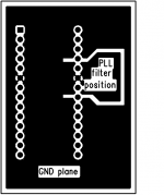
split versus not split
You could use the split thing to some level.
Example :
Your PLL for the DIR1701/1703. You have 3 pins : AVDD (pin 24),AGND (pin 23) and FILT(pin 22).
Your DGND is placed on (pin 6).
Then look at the image. It is not split up that much. Normaly you would take you AVDD from your DVDD through a filter (ferritbead, RC filter ... )
Sonny
PS : I forgot to say that this is a way of prevent digital current loops flow through the PLL filter wich is your ciruit needed to make a stable and jitter "free" clock. This is not possible when you do not make such thing to you PCB design.
Attachments
Fun with Groundplanes
Read the notes at www.analog.com on the AD8307 logarithmic converter. If you don't ground this baby correctly you can have a very nice wide band receiver (with great dynamic range!). I liked the comment on www.sigcon with respect to fixing a groundplane problem -- if you are succesful this becomes your job description. I also read on one of the analog sites the tale of finding emi problems by using an inexpensive (aka very cheap) a.m. radio and passing it over the circuit to find the offending elements.
Read the notes at www.analog.com on the AD8307 logarithmic converter. If you don't ground this baby correctly you can have a very nice wide band receiver (with great dynamic range!). I liked the comment on www.sigcon with respect to fixing a groundplane problem -- if you are succesful this becomes your job description. I also read on one of the analog sites the tale of finding emi problems by using an inexpensive (aka very cheap) a.m. radio and passing it over the circuit to find the offending elements.
An article which addresses multiple ICs requiring quiet grounds:
http://www.sigcon.com/articles/edn/multipleadc.htm
I am planning on going with the "multiple moat" approach and use differential outputs, avoiding any reference to chassis (or external) ground.
Does this change your single-ground recommendation Harry?
Your bypassing note is well taken Jocko.
http://www.sigcon.com/articles/edn/multipleadc.htm
I am planning on going with the "multiple moat" approach and use differential outputs, avoiding any reference to chassis (or external) ground.
Does this change your single-ground recommendation Harry?
Your bypassing note is well taken Jocko.
Did a CD player mod......about 12 years ago with a ground plane. Radiated like mad. Mainly from the analog output jacks.
Jocko
Jocko
Ground plane
A ground plane is the most effective grounding schema for digital circuits in terms of low noise coupling and low EMI. Nothing I have ever read of measured has shown me any reason to believe otherwise. I did EMI reduction as part of my last three jobs and gave a lecture to 150 people on the subject. For a list of good books:
http://www.emiguru.com/bibliog.htm
The following are the best that I have read and are the standard references that I have seen on many engineers bookshelves.
"EMC and the Printed Circuit Board," Mark Montrose, IEEE Press, 1999
"High-Speed Digital Design," Howard W Johnson and Martin Graham, PTR Prentice Hall, 1993
"Introduction to Electromagnetic Compatibility," Clayton Paul, John Wiley & Sons, 1992.
"Noise Reduction Techniques in Electronic Systems," Henry W. Ott, John Wiley & Sons, 1988
H.H.
On the CD player mod, it was necessary to put a cap (few hundred pF) from the output to the ground on the RCA, then put a 0.1 uF from the RCA ground to the chassis ground. With short leads. EMI gone. The analog ground leads acted like a good antenna.
Jocko
Jocko
I' m in the process of designing a PCB (double sided) for a TDA1541 non-oversampling DAC, which will be driven directly from the I2S output of my CD-PRO2 drive. Actually, the DAC will use two TDA1541 dac chips in parallel.
Reading the posts in this thread, the following question arose: should I use a single or dual (A + D) ground plane? The board will not include other chips except the two TDA1541 dac chips. According to the posts, the dac chip should be considered as analog part and should rest entirely on the analog ground plane. But, on the other hand, this chip has already two seperate ground pins, one analog and one digital ground. If the designer of the chip chose to have two different ground pins, why should I consider them as a single ground point?
So,which way to go, single or double ground plane?
- Status
- Not open for further replies.
- Home
- Source & Line
- Digital Source
- Questions re: digital grounding