Hello everybody,
I have a question regarding common source Amplifier outputs. As these have thier sources at thier supply, even a small ripple in the supply voltage causes them so conduct more. This does not produce an output signal however as the NFB of the amplifier corrects the Offset and centers it.
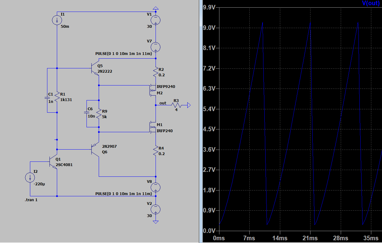
The same cant be said for the cross conduction that is happening. As the Feedback loop does not see the current between the Mosfets when its not producing an offset voltage, this causes the bias to drift and also causes heating of the Mosfets due to several amps cross conduction. I made a MWE of an OPS/VAS to illustrate my question*:

V7/8 simulate 1 V of Supply ripple. Without a feedback loop this causes a massive Offset of over 9 V. The lower fet ceases conduction completely
My question is now, how is this adressed in an Amp? I did not find many amps that use this ops and only one by Nelson Pass mentioned that it needs a regulated supply. Are there other methods for preventing cross conduction in this principle? Is this the reason why its so seldomly seen? Is this topic discussed elswhere? I had a hard time finding annything on that.
Thanks for your time and have a nice day =)
*as I said just for Illustration I do not intend to use a 2N2222 for a fet driving stage...
I have a question regarding common source Amplifier outputs. As these have thier sources at thier supply, even a small ripple in the supply voltage causes them so conduct more. This does not produce an output signal however as the NFB of the amplifier corrects the Offset and centers it.
The same cant be said for the cross conduction that is happening. As the Feedback loop does not see the current between the Mosfets when its not producing an offset voltage, this causes the bias to drift and also causes heating of the Mosfets due to several amps cross conduction. I made a MWE of an OPS/VAS to illustrate my question*:
V7/8 simulate 1 V of Supply ripple. Without a feedback loop this causes a massive Offset of over 9 V. The lower fet ceases conduction completely
My question is now, how is this adressed in an Amp? I did not find many amps that use this ops and only one by Nelson Pass mentioned that it needs a regulated supply. Are there other methods for preventing cross conduction in this principle? Is this the reason why its so seldomly seen? Is this topic discussed elswhere? I had a hard time finding annything on that.
Thanks for your time and have a nice day =)
*as I said just for Illustration I do not intend to use a 2N2222 for a fet driving stage...
Attachments
Last edited:
You may wanna follow tha ska-150 discussions on all platforms: https://www.avforums.co.za/index.ph...HPSESSID=hscd0t2sbn40vic8s256j3p3q6#msg853555
https://www.diyaudio.com/community/threads/ska-gb150d-now-public-domain.238593/
https://www.diyaudio.com/community/threads/ska-gb150d-now-public-domain.238593/
Well one thing is certain, that's not a common drain circuit...
Hi Mark,
I encountered a similar thing in a post that I queried for clarification here https://www.diyaudio.com/community/threads/cancelling-memory-distortion.25428/post-6603077
From Post 60 https://www.diyaudio.com/community/threads/cancelling-memory-distortion.25428/post-6603126 a "common source output in a power amp" means a common source stage as it is usually understood is being used as the output stage of a power amp.
Now back to this thread. It begins
Therefore the question in Post 1 by 3eepoint should have been:
I have a question regarding common source Amplifier output stages. As these have their sources at their supplies.
Also the thread title should be changed to: ... common source ...
At least that's my opinion.
What appears to be causing confusion with some is a push-pull output stages with common sources to their supplies also usually have drains common to the output terminal! Hence the description as "a common drain output amplifier". I think we should stick to the traditional descriptions to avoid confusion.
I encountered a similar thing in a post that I queried for clarification here https://www.diyaudio.com/community/threads/cancelling-memory-distortion.25428/post-6603077
From Post 60 https://www.diyaudio.com/community/threads/cancelling-memory-distortion.25428/post-6603126 a "common source output in a power amp" means a common source stage as it is usually understood is being used as the output stage of a power amp.
Now back to this thread. It begins
and the circuit shown has their sources to the supplies so it is a common source output stage as you say.I have a question regarding common drain Amplifier outputs. As these have thier sources at thier supply
Therefore the question in Post 1 by 3eepoint should have been:
I have a question regarding common source Amplifier output stages. As these have their sources at their supplies.
Also the thread title should be changed to: ... common source ...
At least that's my opinion.
What appears to be causing confusion with some is a push-pull output stages with common sources to their supplies also usually have drains common to the output terminal! Hence the description as "a common drain output amplifier". I think we should stick to the traditional descriptions to avoid confusion.
Hi everybody,
sorry for going silent. Had other stuff to do but now have some free time.
Again, sorry, for butching up the correct naming. I will try to get the titel changed if possible. Already corrected it in the post itself to, as Ian already said, avoid confudion.
@dreamth
Thanks for the hints! As far as I see, the trick is to drive the fet from a bjt collector with a resistor to the Mosfet supply. This kinda works as a controlled current soure and keeps the Voltage Drop across the Resistor and thus the Mosfet Vgs somewhat constant.
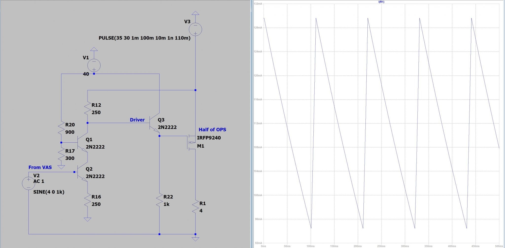
I tried to make up a circuit that incorporates that an came up with this:

To keep it simple its only the upper Half and the VAS is missing. Q1/2 are the mentioned controlled current source. Q2 is cascoded with Q1 to increase its supression of changing Voltages. It reduces the Bias modulation to a 30 somewhat mA range. While not perfect it at least does not selfdestruct directly.
Did I get the idea right or is there a better way of doing this?
sorry for going silent. Had other stuff to do but now have some free time.
Again, sorry, for butching up the correct naming. I will try to get the titel changed if possible. Already corrected it in the post itself to, as Ian already said, avoid confudion.
@dreamth
Thanks for the hints! As far as I see, the trick is to drive the fet from a bjt collector with a resistor to the Mosfet supply. This kinda works as a controlled current soure and keeps the Voltage Drop across the Resistor and thus the Mosfet Vgs somewhat constant.
I tried to make up a circuit that incorporates that an came up with this:
To keep it simple its only the upper Half and the VAS is missing. Q1/2 are the mentioned controlled current source. Q2 is cascoded with Q1 to increase its supression of changing Voltages. It reduces the Bias modulation to a 30 somewhat mA range. While not perfect it at least does not selfdestruct directly.
Did I get the idea right or is there a better way of doing this?
Hi 3eepoint,
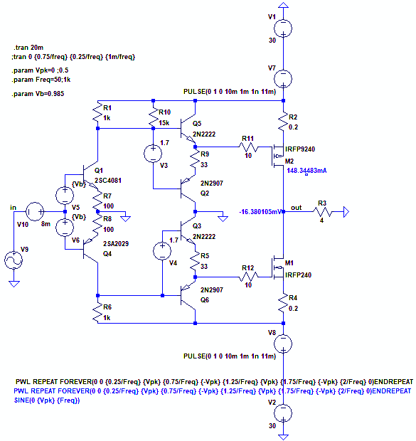
Here's what I'd do for common source to your original basic idea

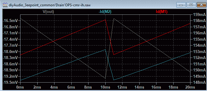
The drivers are made push-pull. Rail ripple is shown below (3mV in Vout and 4mA in drain currents):

The level shifters are Q1 and Q4. The bias voltages (V5,V6) need to be linked to Q1 and Q4. Bias voltages V3 and V4 are not critical for biasing of the MOSFETs.
R10 is optional to trim the gm difference between the p and n-MOSFETs.
With IRFP MOSFETs you need thermal compensation of the idle current. It cannot be done using the level shift bias spreader because of the voltage gain (x10) of this stage giving a way too large temp.co. One option is to add a thermistor across R1 and another across R6 and placed on the MOSFET drain leg. The thermistor value is chosen to give the right compensation - the value depends on the mounting and heatsink arrangement.
Here's what I'd do for common source to your original basic idea
The drivers are made push-pull. Rail ripple is shown below (3mV in Vout and 4mA in drain currents):
The level shifters are Q1 and Q4. The bias voltages (V5,V6) need to be linked to Q1 and Q4. Bias voltages V3 and V4 are not critical for biasing of the MOSFETs.
R10 is optional to trim the gm difference between the p and n-MOSFETs.
With IRFP MOSFETs you need thermal compensation of the idle current. It cannot be done using the level shift bias spreader because of the voltage gain (x10) of this stage giving a way too large temp.co. One option is to add a thermistor across R1 and another across R6 and placed on the MOSFET drain leg. The thermistor value is chosen to give the right compensation - the value depends on the mounting and heatsink arrangement.
Attachments
Last edited:
- Home
- Amplifiers
- Solid State
- Question regarding Common Drain OPS cross conduction