I'm a little confused by the schematic for Carlos's LM3886 amp (the circuit in this thread).
If I compare the National chip schematic to Carlos's, National shows the Input V+ as being pin 10 and the Input V- as pin 9. However Carlos's diagram implies that pin 9 is Input V+ and pin 10 is Input V-
Can someone please clarify the above. I suspect I am missing something fundamental between the difference of inverted and non inverted amps.
Thanks
No,
pin10 is the non-inverting input and pin9 is the inverting input.
Carlos schematic does not number the pins. He simply shows the input signal going to the non-inverting input.
Both National and Carlos are correct.
pin10 is the non-inverting input and pin9 is the inverting input.
Carlos schematic does not number the pins. He simply shows the input signal going to the non-inverting input.
Both National and Carlos are correct.
Another question about the circuit.
Reading schematics is still new to me, but have I correctly interpreted that capacitors C2 and C3 (and their opposite pair) are not connected in parallel?
Thanks
Reading schematics is still new to me, but have I correctly interpreted that capacitors C2 and C3 (and their opposite pair) are not connected in parallel?
Thanks
They are in parallel. Standard practice to use small capacitor paralleled with large one for power filtering.
Ok, so that means that R4 and C7 are connected in parallel to C2 and C3 (although R4 and C7 are connected in series with respect to each other), correct?
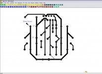
The attached file shows a simple one sided PCB design I've been working on for Carlos's circuit. I've only highlighted C2 and C3, plus V+ and Power Ground tracks. Can you confirm that I have C2 and C3 in parallel - I think I have, but I would like a second opinion.
Thanks
The attached file shows a simple one sided PCB design I've been working on for Carlos's circuit. I've only highlighted C2 and C3, plus V+ and Power Ground tracks. Can you confirm that I have C2 and C3 in parallel - I think I have, but I would like a second opinion.
Thanks
Attachments
Correct. I suggest point to point wiring to get superior performance and eliminate the cost and trouble of circuit board. Here are some good instructions and pictures.
http://dogbreath.de/Chipamps/ThreeResAmp/ThreeResAmp.html
http://dogbreath.de/Chipamps/ThreeResAmp/ThreeResAmp.html
I suggest PCB to get superior performance and save the trouble of instable mechanics and shorts due to loose pins and wires touching each other. As an add-on you can expect easier mounting and maintenance.
On the board move C3 as close as possible to the IC pins. Better still is to leave it out in the board and solder it directly to the pins from below the board.
On the board move C3 as close as possible to the IC pins. Better still is to leave it out in the board and solder it directly to the pins from below the board.
You can have the best of both worlds with this chips, as the original Gaincard proved. Use p2p wiring and use a pcb.
In order to do that you will have to:
1) Solder parts on both sides of the board.
2) Or use a double-sided pcb.
The main thing is to keep distances as short as possible.
In order to do that you will have to:
1) Solder parts on both sides of the board.
2) Or use a double-sided pcb.
The main thing is to keep distances as short as possible.
- Status
- Not open for further replies.
- Home
- Amplifiers
- Chip Amps
- Question about Carlos's LM3886 circuit