Hi everyone,
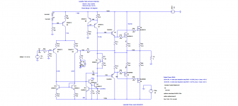
I've simulated this amplifier using quasi complementary output stage, I don't pretend to build it, it's just to compare the characteristics of a typical complementary output amplifier, with this old technic. This design has some problems, because of the assymetrical load on VAS, but this can be almost solved with the added resistor R28, this resistor seems to decrease the output swing and why this happens? The amplifier saturates for lower Vin voltages, compared to the complementary OPS. I've also another question, the CMiller capacitor in this topology should be placed between the output of the LTP and the output of the amplifier, because of the gain in the PMOS emulated transistor (because it is an emitter follower), but in the simulation conventional compensation seems to work, why?
I've made those two amplifiers, the collector resistors are intended to use with Michael Kiwanuka's protection systems. Which one of the attached designs is better?
Another question, why almost IC audio amps use this old type of OPS? Transistor size? Bad complementary matching?
Thank you very much for your attention,
Best regards,
Daniel Almeida
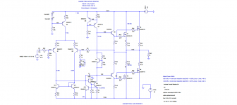
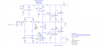
Attachments
-
 MOSFET2.png31.1 KB · Views: 220
 -
 MOSFET2_quasi_complementary1.png31.5 KB · Views: 213
 -
 MOSFET2_quasi_complementary2.png31.3 KB · Views: 206
 -
MOSFET2.asc8.9 KB · Views: 62
-
MOSFET2_quasi_complementary.asc9 KB · Views: 58
-
MOSFET2_quasi_complementary2.asc9 KB · Views: 80
-
Cordell Models.txt11.8 KB · Views: 57
Read up on the modifications introduced by Baxandall, JLH and others.
diode and resistor and capacitor added to the lower driver emitter to mimic the load on the upper driver.
diode and resistor and capacitor added to the lower driver emitter to mimic the load on the upper driver.
Hello Andrew and thank you for your reply,
I've read about Peter Baxandall's diode, that is used to increase the voltage on the lower driver from about 0.6-0.7V to 1.2-1.4V, but I think that this can be achieved with only one resistor, if the resistor as a drop of about 0.6-0.7V, as about the capacitor, I don't know exactly what that improvement does, but I think that this can be used to lower the chance of oscillations, caused by the assymetrical loading and by the gain that could appear at the lower side transistor, that is a source/emitter follower, but this amplifier seems to be stable only with Miller capacitance, but has I've said, I've never made anything like this so I don't know exactly it's behaviour, this things I'm saying are based on suppositions, on Bob Cordell's and Randy Slone's books and LTSpice/TINA simulations.
Best regards and thank you once more,
Daniel Almeida
- Status
- Not open for further replies.