What do you mean by 'Driver A' ?
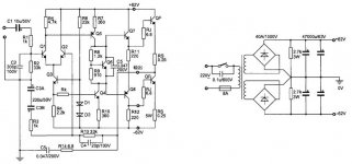
The output stage is a conventional quasi stage. The upper two NPN's (Q7 and QF) form a standard driver + output. The lower PNP driver (Q8) and its associated NPN output device (also QF) form a quasi PNP output device and driver. Pulling the base of TR8 negative turns the transistor on. That in turn develops a voltage across R12 which turns on the lower QF. It behaves very much like two PNP devices.
The output stage is a conventional quasi stage. The upper two NPN's (Q7 and QF) form a standard driver + output. The lower PNP driver (Q8) and its associated NPN output device (also QF) form a quasi PNP output device and driver. Pulling the base of TR8 negative turns the transistor on. That in turn develops a voltage across R12 which turns on the lower QF. It behaves very much like two PNP devices.
Thank Mooly.
I find it strange the R11 between emisor Q7 and Q8. Drivers are in class A? I do not see the classic organization of drivers as in quasi as Nap140, ArcamA60 and other.....This organization (drivers and output) works well?
I find it strange the R11 between emisor Q7 and Q8. Drivers are in class A? I do not see the classic organization of drivers as in quasi as Nap140, ArcamA60 and other.....This organization (drivers and output) works well?
Hi,
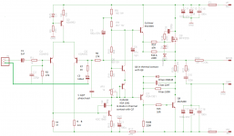
Adding a so called "baxandall diode" is generally a very good idea.

In this case add 220R with a parallel diode to the base of the lower driver.
It makes the output biasing far more symmetric and lowers x/o distortion.
rgds, sreten.
Adding a so called "baxandall diode" is generally a very good idea.
In this case add 220R with a parallel diode to the base of the lower driver.
It makes the output biasing far more symmetric and lowers x/o distortion.
rgds, sreten.
Last edited:
Thank Mooly.
I find it strange the R11 between emisor Q7 and Q8.
Looking more closely and I believe there is an error in the diagram and that it would not work as shown. It should be like this.

Connected as it was is valid if the lower output device were PNP and in this configuration it allows each of the drivers to actively pull down (or up) the other drivers base and so aid a faster turn off.
Yes an error.
Seeing sretens post above reminded me of a previous thread (post #7):
http://www.diyaudio.com/forums/soli...er-quasi-complimentary-stage.html#post4126274
Seeing sretens post above reminded me of a previous thread (post #7):
http://www.diyaudio.com/forums/soli...er-quasi-complimentary-stage.html#post4126274
My quasi amp also cap 220pf on collector to base on Q5.
I found I just needed C3A and not C3B.
I found the idle voltage across C3A to be negative by a couple of volts.
This is because drive into output transistors is not biased around zero volts.
The bias voltage is offset due to different types of output transistor driver.
I found I just needed C3A and not C3B.
I found the idle voltage across C3A to be negative by a couple of volts.
This is because drive into output transistors is not biased around zero volts.
The bias voltage is offset due to different types of output transistor driver.
This scheme found it on the internet. I am not technical, I know the quasi topology. Only caught my intention R11 between the emitters of drivers. It is a disastrous scheme. There are many errors.
Thanks
Thanks
Only caught my intention R11 between the emitters of drivers. It is a disastrous scheme. There are many errors.
Thanks
My amps drivers have 220R resistors from drivers to output instead of R11.
An externally hosted image should be here but it was not working when we last tested it.
nigelwright7557.
Very interesting their scheme
In the thread "Very simple quasi complimentary MOSFET amplifier"(Ranchu32) in the post 162, Ilimzn says "Now, becasue of the unusual nature of a BJT CFP/MOSFET combination, there is actually more that can be done to simplify the design. For one, the R-C-D parallel combo is not necessary. This would be used if the top was a BJT darlington, and it's used to make the crossover region more symmetrical, because for the CFP it's much narrower than that of the darlington. In the case of this amplifier, it's very difficult to do this since the devices are so different. However, it is possible to narrow the Vgs range the top MOSFET works in, by excluding the source ressitor. At the same time, the 'emitter' resistor of the CFP mentioned above should be increased, perhaps to 0.47ohms"
My question is if necessary diode Baxandall in his scheme and why has no capacitor in parallel with R12?
nigelwright7557.My question is if necessary diode Baxandall in his scheme and why has no capacitor in parallel with R12?
The diode pretty much acts as a short so a capacitor across it isn't needed.
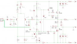
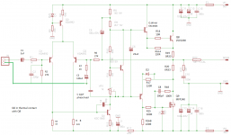
Here I have two quasi hybrid schemes. What is your opinion?
The second circuit wont work.
The drive is the wrong way around for the lower mosfet.
It needs a inverting stage to drive the mosfet.
The first circuit is a little odd with bipolar and a mosfet on the output.
Second circuit: to work has to be PMOS or with driver?
It needs an inverter stage on the lower mosfet input.
- Status
- Not open for further replies.
- Home
- Amplifiers
- Solid State
- Quasi AB driver A