Hello,
I wonder why there are curvy PCB traces found in OPPO BDP-83 Blu-ray Player PCB as attached.😕 The picture is from http://www.oppodigital.com/blu-ray-bdp-83se/images/Blu-ray-BDP-83_Board_hr.jpg. Actually, I can find similar traces in computer motherboard.
Thanks in advance.
I wonder why there are curvy PCB traces found in OPPO BDP-83 Blu-ray Player PCB as attached.😕 The picture is from http://www.oppodigital.com/blu-ray-bdp-83se/images/Blu-ray-BDP-83_Board_hr.jpg. Actually, I can find similar traces in computer motherboard.
Thanks in advance.
Attachments
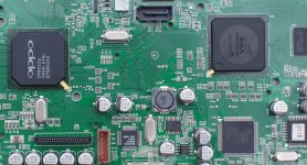
at those speeds the chips in your player are running at, timing becomes so important, that the traces for data lines must be almost equal in length to prevent phase-shifts
Now I notice the SATA connector on the board... What is doing there, I was thinking that only 93 has SATA HDD connection?
Last edited:
At first I thought the width of the trace varied smoothly. This is to prevent signal reflections from changes in impedance.
But what I see here looks like you have high-speed digital signals going down these traces, and they all need to arrive at the same time. So, if some paths would be shorter than others, you curve them around so they all line up in the end.
But what I see here looks like you have high-speed digital signals going down these traces, and they all need to arrive at the same time. So, if some paths would be shorter than others, you curve them around so they all line up in the end.
Heavyweight PCB CAD packages can do that automatically: Nets can be tagged / paired as requiring equal path lengths and an 'autorouter' will push and shove other traces out of the way to make the space.
This is often seen with high speed pairs into differential line receivers.
This is often seen with high speed pairs into differential line receivers.
Skew control, have a look at the requirements for DDR memory, one of the more critical interfaces on a PCB. It requires a router that can handle high speed designs, you have to enter the max skew as either a time or a length. It cannot usually be done manually as quite often you are matching signals within one group to signals within other groups and then to clocks. To make matters worse, when this is on a board the board quite often has to be impedance matched, so each signal layer has to be closely tied to a ground plane for return currents.
Its most noticable on mother boards between the CPU, interface chips and the DDR sockets.
Its most noticable on mother boards between the CPU, interface chips and the DDR sockets.
Not being overly familiar with modern PCB-design (to put it mildly), the pic above got me into asking myself , whether the curvy sections of the traces in post #1 would (also ?) be used as on-PCB inductors.
I found a more revealing sample of this there:
http://www.thel-audioworld.de/module/siebung/stvu.jpg
So could this also be the case with the Oppo-PCB ?
Greez & Thanks
SigFiire
I found a more revealing sample of this there:
http://www.thel-audioworld.de/module/siebung/stvu.jpg
So could this also be the case with the Oppo-PCB ?
Greez & Thanks
SigFiire
No is the short answer, its more prone to artifacts such as mutual crosstalk, the general rule being use 3 tiems the track to track spacing between the consatinas where possible. If you want to create inductors on a PCB look up "planar transformers", you can do all sorts of funky things.
I'd say the pattern on that PCB would create more capacitive coupling between the planes than inductive.
Rememeber it is signal rise times that cause signal integrity problems, use the slowest possible rise time for any signals to minimise problems.
I'd say the pattern on that PCB would create more capacitive coupling between the planes than inductive.
Rememeber it is signal rise times that cause signal integrity problems, use the slowest possible rise time for any signals to minimise problems.
Last edited:
- Status
- Not open for further replies.
- Home
- Source & Line
- Digital Source
- Q: Why curvy PCB traces?