Hi,
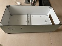
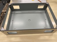
I'm going to test a new vacuum tube amp build, and would like to avoid problems with 50Hz and HF noise I had in the past. Power supply and amp prototype will be housed in separate boxes made with 3mm thick Neobond (porous plastic with 0.5mm aluminum on both sides). Neobond is surprisingly light and sturdy, is easy to process (mill, drill, etc.). Aluminium foil on both sides will serve as EM shielding. Foil on outer side remain intact, yet on inner is being cut with V-mill in order to bend sheet into a box. So where necessary I scraped coating in order to restore conductivity (e.g. on corners with aluminum brackets of 2020 type, DIN rail mount, etc.).
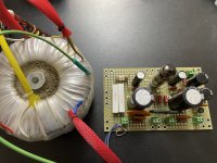
Power supply is assembled on prototyping PCB, stacked type 2xHV (220V toroidal transformer, secondary 2x159V, plus additional 42V/35V for adjusting output voltage, 60V BIAS, 3x6.3V filament). PS output terminals will be DIN rail splice quick connect type.
Since toroidal transformer supports up to 8A on each 6.3V tap, and will power up only 1 channel, I plan to power all vacuum tubes from single 6.3V tap.
For safety reason amp PCB will be mounted on additional riser plastic plate, not on the bottom of the box directly (further away from metallized surface).
Now the question: how do you recommend to make routing between these parts of the whole assembly: 220V power line ground, power transformer Faraday shield, power supply chassis, amplifier chassis, BIAS GND, amplifier GND, filament artificial middle tap (from 2 x 100...200 Ohm resistors). IMHO HV power and BIAS GND must be connected near terminal of PS PCB board (or may be amp PCB?).
Photos of some parts attached. Amp itself is on early assembly stage so there is nothing to show right now.
Thanks in advance for any help.
I'm going to test a new vacuum tube amp build, and would like to avoid problems with 50Hz and HF noise I had in the past. Power supply and amp prototype will be housed in separate boxes made with 3mm thick Neobond (porous plastic with 0.5mm aluminum on both sides). Neobond is surprisingly light and sturdy, is easy to process (mill, drill, etc.). Aluminium foil on both sides will serve as EM shielding. Foil on outer side remain intact, yet on inner is being cut with V-mill in order to bend sheet into a box. So where necessary I scraped coating in order to restore conductivity (e.g. on corners with aluminum brackets of 2020 type, DIN rail mount, etc.).
Power supply is assembled on prototyping PCB, stacked type 2xHV (220V toroidal transformer, secondary 2x159V, plus additional 42V/35V for adjusting output voltage, 60V BIAS, 3x6.3V filament). PS output terminals will be DIN rail splice quick connect type.
Since toroidal transformer supports up to 8A on each 6.3V tap, and will power up only 1 channel, I plan to power all vacuum tubes from single 6.3V tap.
For safety reason amp PCB will be mounted on additional riser plastic plate, not on the bottom of the box directly (further away from metallized surface).
Now the question: how do you recommend to make routing between these parts of the whole assembly: 220V power line ground, power transformer Faraday shield, power supply chassis, amplifier chassis, BIAS GND, amplifier GND, filament artificial middle tap (from 2 x 100...200 Ohm resistors). IMHO HV power and BIAS GND must be connected near terminal of PS PCB board (or may be amp PCB?).
Photos of some parts attached. Amp itself is on early assembly stage so there is nothing to show right now.
Thanks in advance for any help.
Attachments
1. Hum and High Frequency Noise have lots of causes.
Know all the causes, or you may get more than you need.
What kind circuits is your amplifier going to be?
Single Ended 2 stage, SE 3 stages?
Push Pull - concertina phase inverter; long tailed pair phase inverter; paraphase phase inverter.
All Indirect heated, or DHT? DHT with DC power?
B+ Power supply choke input or cap input.
Is the first local ground loop small and controlled?
With cap input, the high frequency is large if the ground loop is not controlled.
Is there adequate B+ filtering (ripple controlled)?
Are the power transformer, filter choke orientation 90 degrees different than the output transformer orientation.
Is there adequate space between the power transformer and choke far enough away from the output transformers.
Are the filaments of indirectly heated tubes properly bypassed and DC elevated if necessary?
Are you using a magnetic steel chassis, No, you are not.
Are the input connectors and input stages ground loops controlled?
Ground loop control is an art, but is mostly a science.
Just to mention a few causes of hum and noise.
2. Please post a schematic diagram, we may be able to point a few areas that need particular attention.
Faraday cages work well for capacitive coupling. At mains frequency you're mostly looking at inductive coupling. Minimize the loop areas of sensitive circuitry.
Tom
Tom
This build is 100% new, so it doesn't have (yet) problems present in the past with previous assemblies. Schematic of the amplifier attached (its a HK Citation II). Power supply schematic is so standard there is nothing to show (photo attached to 1st post). No filter inductor, 560uF HV cap, 2000 uF BIAS filter cap, + ceramic capacitors for HF noise. Vacuum tube SG2P only as indicator of HV power on. Large ceramic resistors for discharging PS filter caps.
The main question was how you would suggest to wire amp signal ground / chassis ground of these components of the assembly:
220V power line ground
power transformer Faraday shield
power supply chassis
amplifier chassis
BIAS GND
amplifier GND
filament artificial middle tap (from 2 x 100...200 Ohm resistors).
Junction of amp GND and BIAS GND on the power supply PCB or amplifier PCB ?
Thanks in advance.
Attachments
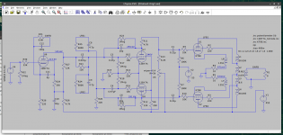
Is that schematic the real Original HK Citation II?
Or, is it a Modified Circuit that was based on a HK Citation II?
Thanks!
Or, is it a Modified Circuit that was based on a HK Citation II?
Thanks!
Its LTSpice simulation, there almost no changes from the original except another transformer with CFB. And its better readable compared to old scanned original.
Its downloadable on another thread here:
https://www.diyaudio.com/community/threads/failed-ltspice-simulation-of-hk-citation-ii.392308/
Its downloadable on another thread here:
https://www.diyaudio.com/community/threads/failed-ltspice-simulation-of-hk-citation-ii.392308/
There's a few rules regarding layout, though they aren't rules as such, but guidelines.
1) Keep all wiring as short as possible
2) All grounds to C1's negative terminal
3) High current stages go first, IE nearest to C1, with subsequent stages grounded in order of current consumption.
4) Chassis ground grounded to chassis at one place only, usually at the IP socket or at V1's valve base
5) If signal wires cross a wire carrying AC current do so at 90 degrees to it.
6) Heater wiring tucked into chassis corners, don't loop wires round the valve base and use a humbucker pot if needed.
I'm sure there's others but for a good guide see Merlins site - http://www.valvewizard.co.uk/Grounding.html for instance. Regarding HF interference or stray EMF it can get into your amp in so many ways as can other spikes and pops,via the air, via the mains, through speaker leads etc, you could fit a LPF on the IP, something like a 2k2 & a 2n2 which rolls off everything over 30khz ish. Also make sure your OPT's and mains tfmr are at 90 degress to each other.
Where things get tricky is if you have a separate power supply and two monoblocks say, I encountered significant issues with the mains earth. you can also encounter ground loop issues.
Lastly on a first build don't attach components by wrapping them round turret tags etc, chances are you'll have to change component values or resite grounds etc. Go over your work a few times with a magnifying glass if needed to check and re-check you have the right components in the right place and solder joints are good.
Andy.
Ok, thanks a lot, excellent article !I'm sure there's others but for a good guide see Merlins site - http://www.valvewizard.co.uk/Grounding.html for instance.
Andy.
- Home
- Amplifiers
- Tubes / Valves
- Q: Prototype Build - Routing Ground and Other Assembly Considerations