A few years ago, I presented a small resonant converter, the Q-conv:
https://www.diyaudio.com/forums/power-supplies/286078-resonant-hv-converter-conv-post4599222.html
This version uses the same principles and has similar features, applications and specifications, but it is somewhat simpler, thanks to the single-ended power section and a minimalist control circuit.
The resonant principle allows a "soft" operation, without large amplitude transients, and does not require custom magnetics: a standard, two-terminal choke is sufficient, and in applications where non-isolated input and output grounds are acceptable, it provides a simple and quiet solution.
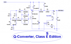
This is the circuit:

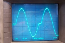
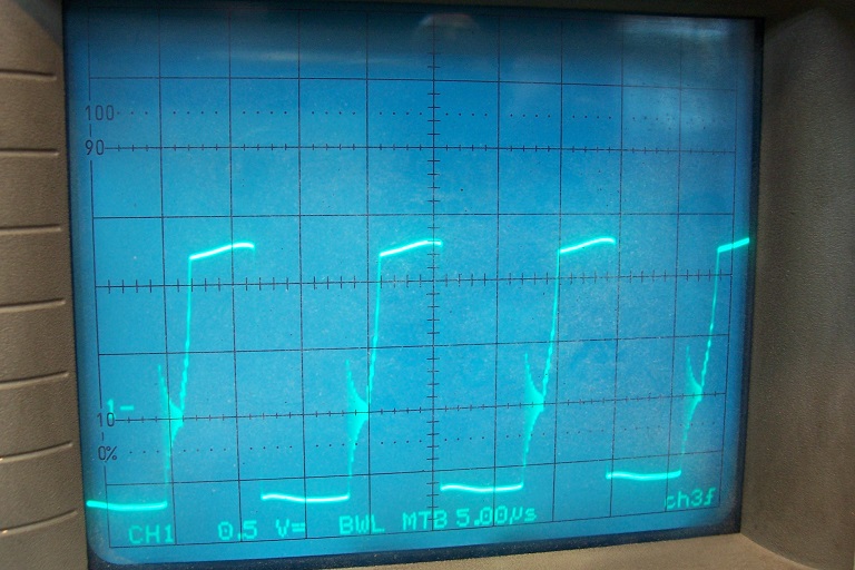
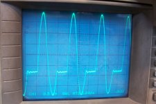
And this is the output waveform (unloaded) on the tank circuit:

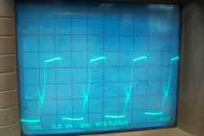
This is the same waveform under full load conditions:
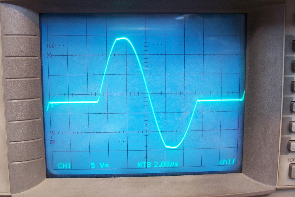
The waveform is essentially a sequence of sinewave cycles, separated by variable-length zero-crossing "pauses".
In addition, when the output is loaded, the rectifying diodes slightly clip the tops, but compared to a conventional, switching converter it remains very benign.
With the values indicated, the operating frequency is comprised between 50 and 80kHz.
The circuit is designed for an output power of 10~20W, but there is no lower limit. Going higher would also be possible, but it is probably not advantageous because of the limited efficiency: 74% @15W.
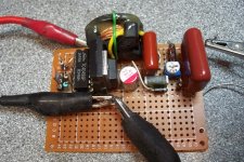
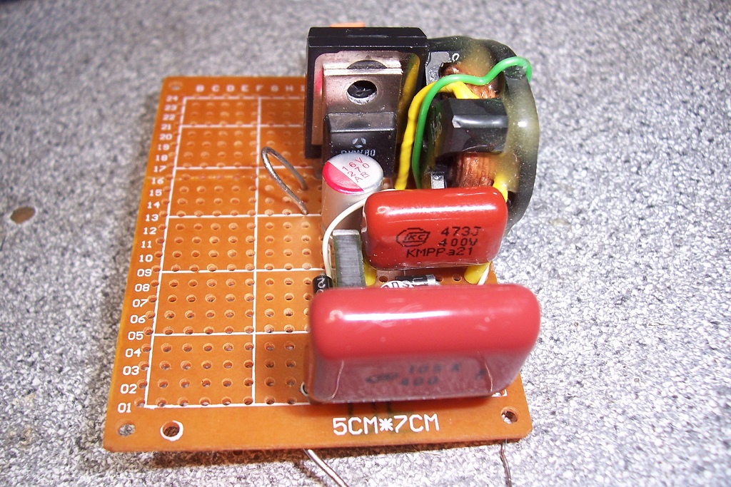
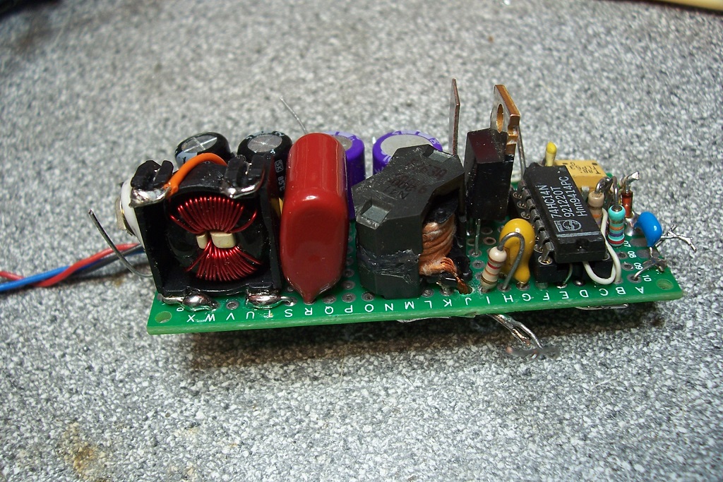
Here is a pic of my prototype:

The inductor is based on an unholy hybrid between a cross-core and an old potcore, because I didn't have a suitable standard inductor available, but basically, any standard 56µH/6A power choke would work (and would have lower losses than this one)
https://www.diyaudio.com/forums/power-supplies/286078-resonant-hv-converter-conv-post4599222.html
This version uses the same principles and has similar features, applications and specifications, but it is somewhat simpler, thanks to the single-ended power section and a minimalist control circuit.
The resonant principle allows a "soft" operation, without large amplitude transients, and does not require custom magnetics: a standard, two-terminal choke is sufficient, and in applications where non-isolated input and output grounds are acceptable, it provides a simple and quiet solution.
This is the circuit:
And this is the output waveform (unloaded) on the tank circuit:
This is the same waveform under full load conditions:
The waveform is essentially a sequence of sinewave cycles, separated by variable-length zero-crossing "pauses".
In addition, when the output is loaded, the rectifying diodes slightly clip the tops, but compared to a conventional, switching converter it remains very benign.
With the values indicated, the operating frequency is comprised between 50 and 80kHz.
The circuit is designed for an output power of 10~20W, but there is no lower limit. Going higher would also be possible, but it is probably not advantageous because of the limited efficiency: 74% @15W.
Here is a pic of my prototype:
The inductor is based on an unholy hybrid between a cross-core and an old potcore, because I didn't have a suitable standard inductor available, but basically, any standard 56µH/6A power choke would work (and would have lower losses than this one)
Attachments

The circuit works by first building-up, then maintaining oscillations in the resonant circuit.
It does so by injecting a small amount of energy after each cycle has ended, exactly at the zero-crossing instant.
If the switching is performed when the voltage across the switching element (the MOSFET) is zero, the switching losses vanish completely: that's the principle of class E operation.
This normally requires a great timing accuracy, to perfectly synchronize the master-oscillator's frequency to the pseudo-period of the passive tank circuit.
Failing to do so would result in huge switching losses, and/or an output voltage out of control, with oscillations building up to destruction, or dying out completely.
Achieving such a result with a crude, PWM'ed CMOS oscillator requires a two-tier strategy:
To avoid a zero-crossing detector circuit, the start of the conduction period is determined by a natural switching element, the free-wheeling diode D1.
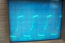
The MOS is turned-on well before the zero-crossing, at some point during the negative swing of the cycle:
This pic shows the output waveform and the gate-drive signal:
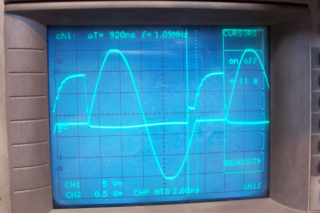
The cursors materialize the advance of the turn-on signal over the actual conduction period, which can only begin when the diode becomes forward-biased.
The timing isn't critical at all: the drive signal can become active at any point during the negative half-cycle without changing the operation of the circuit.
Now that the starting instant of the replenishment period has been accurately determined, the end of the conduction also needs to be defined: that's where the PWM comes into play.
The closed loop control of the active period of the oscillator through the zeners and trimmer ensure an exact balance of the energies injected and extracted from the tank circuit.
The resulting circuit is simple, robust and very accurate, without requiring precision components or precise trimming.
It does have a big drawback though: the freewheeling diode does wonders, but it also consumes a significant amount of power, due to its forward voltage.
All of the supply current has to pass through the diode, meaning a 1V average loss and a non-compressible 8.5% efficiency penalty to begin with (for a 12V supply).
For lower output voltages, a schottky diode would be usable and ~halve the losses, but here the blocking voltage needs to be at least 150V, which excludes "plain-vanilla" schottky diodes stopping at 100V (there are now devices capable of hundreds of volts, but I prefer to keep the circuit low-tech and accessible).
A conventional epitaxial diode like the BYW80 takes the lion's share of the losses.
The beauty of the class E scheme is that it does not require fast-switching components: that is true for the switching element, the free-wheeling diode (it just requires a fast forward recovery, which is the case even for relatively slow diodes) and the rectification diodes: thanks to the sine wave-shape, only moderately fast diodes are sufficient, and even if they "stick" a little during the recovery, it is inconsequential: they see a capacitance on both their input and output, meaning a switching noise confined to just the rectification loop.
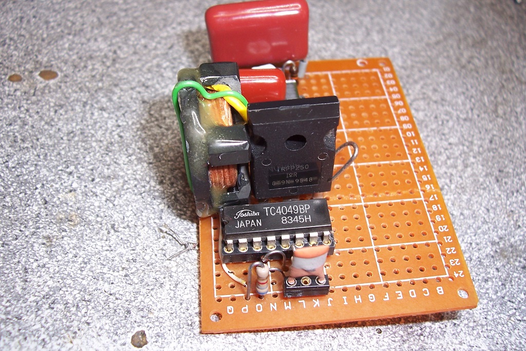
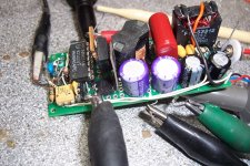
Here are some more pics of the prototype:
It does so by injecting a small amount of energy after each cycle has ended, exactly at the zero-crossing instant.
If the switching is performed when the voltage across the switching element (the MOSFET) is zero, the switching losses vanish completely: that's the principle of class E operation.
This normally requires a great timing accuracy, to perfectly synchronize the master-oscillator's frequency to the pseudo-period of the passive tank circuit.
Failing to do so would result in huge switching losses, and/or an output voltage out of control, with oscillations building up to destruction, or dying out completely.
Achieving such a result with a crude, PWM'ed CMOS oscillator requires a two-tier strategy:
To avoid a zero-crossing detector circuit, the start of the conduction period is determined by a natural switching element, the free-wheeling diode D1.
The MOS is turned-on well before the zero-crossing, at some point during the negative swing of the cycle:
This pic shows the output waveform and the gate-drive signal:
The cursors materialize the advance of the turn-on signal over the actual conduction period, which can only begin when the diode becomes forward-biased.
The timing isn't critical at all: the drive signal can become active at any point during the negative half-cycle without changing the operation of the circuit.
Now that the starting instant of the replenishment period has been accurately determined, the end of the conduction also needs to be defined: that's where the PWM comes into play.
The closed loop control of the active period of the oscillator through the zeners and trimmer ensure an exact balance of the energies injected and extracted from the tank circuit.
The resulting circuit is simple, robust and very accurate, without requiring precision components or precise trimming.
It does have a big drawback though: the freewheeling diode does wonders, but it also consumes a significant amount of power, due to its forward voltage.
All of the supply current has to pass through the diode, meaning a 1V average loss and a non-compressible 8.5% efficiency penalty to begin with (for a 12V supply).
For lower output voltages, a schottky diode would be usable and ~halve the losses, but here the blocking voltage needs to be at least 150V, which excludes "plain-vanilla" schottky diodes stopping at 100V (there are now devices capable of hundreds of volts, but I prefer to keep the circuit low-tech and accessible).
A conventional epitaxial diode like the BYW80 takes the lion's share of the losses.
The beauty of the class E scheme is that it does not require fast-switching components: that is true for the switching element, the free-wheeling diode (it just requires a fast forward recovery, which is the case even for relatively slow diodes) and the rectification diodes: thanks to the sine wave-shape, only moderately fast diodes are sufficient, and even if they "stick" a little during the recovery, it is inconsequential: they see a capacitance on both their input and output, meaning a switching noise confined to just the rectification loop.
Here are some more pics of the prototype:
Attachments


Let us have a look at the design/dimensioning. There is more than one way to skin a cat, but this procedure is relatively simple and direct.
Start with the minimum frequency of operation; say 50kHz.
The free-running frequency of the CMOS oscillator is F~=0.42/R*C, thus with R=15K, C=0.42/15000*50000=560pF.
The typical duty-cycle of such an oscillator (with asymetrical gates) is ~0.4.
The time allowed for the pseudo-period of the tank circuit is thus (1-0.4)/50kHz=12µs.
With a supply voltage of 12V, and a useful power of 15W, the average input current will be 15/12*0.7 (assuming an efficiency of 0.7) =1.78A.
The peak current during the replenishment period will be 1.78/0.4=4.5A.
To reach a peak current of 4.5A in the resonant circuit with an output of 150Vpk (there is a voltage doubler), the characteristic impedance of the circuit needs to be 150/4.5=33ohm.
Thus, L=33*12µs/6.28=63µH, and C=12µs/6.28*33=58nF.
This is just the algorithm of the method: in reality, you also need to take safety margins and tolerances into account, but it would be tedious and lenghty to go into every boring detail.
Anyway, the computed values will need to be refined with a simulation (optional) and/or a reality test (required).
The calculations are simplified, and the components are not perfect.
The rms current in the reactive components and the peak currents through the MOS and freewheeling diode will be 4.5A.
Component selection:
The dimensioning procedure provides the basic ratings of the components.
The resonant components are particularly critical, even if they meet the minimal ratings: their losses will determine most of the final efficiency figure.
The inductor is especially important, but even the capacitor will contribute to the losses; polypropylene is the only sensible choice, and a plain-foil type is preferable. I have used a metallized type, and it works, but it costs one or two points of efficiency.
The MOS should have a sufficiently low Rdson, as the losses will be β*Rdson*√0.4.
Whenever possible, the freewheeling diode should be a schottky type; speed is irrelevant, but conduction losses are all-important.
The general bypass cap should be a very low esr type, since the supply current will be heavily pulsed: that is the dark side of this scheme. The output side is soft and gentle, with just minor discontinuities, but the input side will be heavily rippled, and a solid-polymer cap is the ideal choice, to minimize perturbations and optimize the efficiency.
If the DC input is common to other circuits, an inductor should be inserted in the supply line.
Note that the voltage-doubler rectification is not compulsory: for lower voltages, a single diode is sufficient, and the circuit can even provide a negative voltage directly, with just a single diode, as the inversion is performed by the tank circuit.
The same circuit can even do the three at the same time: with the example circuit, you could have the +300V, +150V and -140V simultaneously.
All the outputs will be totally overload-proof, thanks to the resonant principle.
The outputs having a diode link to the + input supply will not be short-circuit proof, as a dead output short will also short the input supply.
In the example, the 300V could be made short-circuit proof by referencing the first diode of the doubler to GND instead of V+.
The only drawback is the loss of 1 point of efficiency; not a big deal.
The example is centered on 300V, because this type of circuit is especially useful for tube supplies, but the principle can be applied to lower voltages (the efficiency will even be improved): phantom supplies, generation of +/-15V from a 12V source, over-the-top supplies for amplifiers, etc.
The low-noise footprint, simplicity, overload resiliency would be great advantages in those applications.
Note that the output is just loosely stabilized, not actually regulated: the loop gain is very low, and if great accuracy is required, a different feedback scheme or a post-regulator should be used
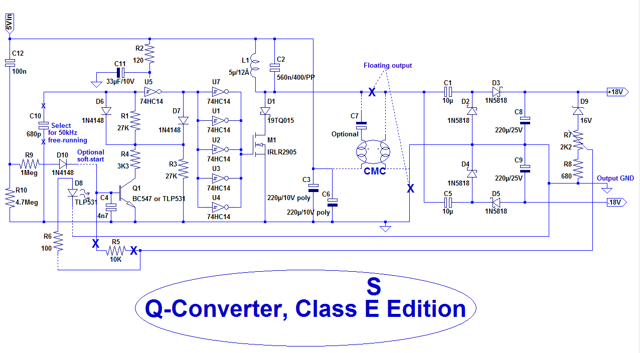
Here is another example, a 5V---> +/-18V, to generate analog supplies in a digital environment (or from a wallwart or USB adapter).
In its most basic form, it is not a particularly attractive proposition: large manufacturers like ADI or TI offer a plethora of DC-DC conversion chips, capable of converting almost anything into anything else, provided it is low-voltage and non-isolated.
They come with examples, reference designs and all you have to do is to copy-paste the layout into your system, use the recommended passives, and you end up with a small, efficient and low noise supply: thanks to the tiny size and typically 4-layer design, emissions can be kept low even though they are traditional, hard-switching types.
Additional filtering components can be added to make them even quieter.
The Q-conv has no edges, just singular discontinuities at the start-stop instants of the sinusoid, meaning it is an order lower compared to hard-switching types, and should therefore have a stealthier noise profile, especially at higher frequencies, at least in theory.
The reality can be somewhat different: the Q-conv will typically be built by hard-boiled DIYers using home-made, single-layer PCB's or PTP and perfboard implementations which cannot compete with a semi-commercial, 4-layer PCB.
The Q-conv doesn't generate large dv/dt's, but the resonance current is large and can radiate a magnetic field in its surroundings. This field will be at a relatively low, but ultrasonic frequency and should cause minimal perturbations, but it will be present.
The cleanliness of a supply can be judged from a number of factors: coarsely, radiated magnetic fields count for ~16%, E-fields for ~16%, differential noise and ripple residues for ~16%.
The elephant in the room is the common-mode noise: in reality, it accounts for more than 50% of the troubles. It is also the most misdiagnosed and the harder to treat.
When a EMC problem appears, the first thing people do is to add more, and more energetic filtering but this has an effect on differential mode only, not CM.
CM perturbations span many decades, from 50/60Hz ground loops and leakage currents to VHF perturbations caused by fast circuits.
For low frequencies, up to 10kHz, isolation (galvanic) is the only realistic option.
For frequencies >1MHz, common-mode chokes are best suited.
In-between, a mix of both is generally necessary.
The difficulty with CMC's is that a member is missing: in differential filters, you have a series impedance and a shunt impedance, but with CM, you only have the series component. The filtered device itself acts as an informal shunt section.
Simple converters, including the Q-conv cannot offer the much-needed isolation without dedicated magnetics, which are a big obstacle for DIYers.
This implementation achieves a very good isolation, without resorting to custom magnetics.
The secret is to use an ordinary CMC as an isolation transformer:
This would be impossible for other types of converters, because of the huge leakage inductance: a flyback converter isolated in such a way would need to dissipate half of its power in snubbers, but a Q-conv swallows it without difficulty.
CMC's have isolation voltages reaching 250V, sometimes more, and for this example (a PE-53912 from Pulse), the I/O capacitance is only ~20pF, and most of this capacitance is "inert", because the primary and secondary are identical and synchronous when connected properly, meaning a zero AC voltage between P and S turns.
Combined with the inherent quietness of the resonant scheme, it allows an ultra-clean supply, using only off-the-shelf components and improvised construction techniques.
This example is designed for +/-18V - 250mA nominal output, but it can go from 17 to 20V, at up to 300mA (other voltages would be possible with a different zener).
Nominal input is 5V, but it works down to 3.5V (with a reduced efficiency) and accepts up to 6V.
A 3.3V version would be possible with another logic family, like the ACMOS.
The efficiency is ~72% for the non-isolated version and 70% for the isolated version.
Most of the losses are caused by the free-wheeling diode.
Some pics of my prototype:

This oscillogram shows the primary side:

This is the secondary; it should be exactly identical with a perfect transformer, but with the CMC, it is barely recognizable.
This is the same with a 150ohm +3.3nF snubber:

In its most basic form, it is not a particularly attractive proposition: large manufacturers like ADI or TI offer a plethora of DC-DC conversion chips, capable of converting almost anything into anything else, provided it is low-voltage and non-isolated.
They come with examples, reference designs and all you have to do is to copy-paste the layout into your system, use the recommended passives, and you end up with a small, efficient and low noise supply: thanks to the tiny size and typically 4-layer design, emissions can be kept low even though they are traditional, hard-switching types.
Additional filtering components can be added to make them even quieter.
The Q-conv has no edges, just singular discontinuities at the start-stop instants of the sinusoid, meaning it is an order lower compared to hard-switching types, and should therefore have a stealthier noise profile, especially at higher frequencies, at least in theory.
The reality can be somewhat different: the Q-conv will typically be built by hard-boiled DIYers using home-made, single-layer PCB's or PTP and perfboard implementations which cannot compete with a semi-commercial, 4-layer PCB.
The Q-conv doesn't generate large dv/dt's, but the resonance current is large and can radiate a magnetic field in its surroundings. This field will be at a relatively low, but ultrasonic frequency and should cause minimal perturbations, but it will be present.
The cleanliness of a supply can be judged from a number of factors: coarsely, radiated magnetic fields count for ~16%, E-fields for ~16%, differential noise and ripple residues for ~16%.
The elephant in the room is the common-mode noise: in reality, it accounts for more than 50% of the troubles. It is also the most misdiagnosed and the harder to treat.
When a EMC problem appears, the first thing people do is to add more, and more energetic filtering but this has an effect on differential mode only, not CM.
CM perturbations span many decades, from 50/60Hz ground loops and leakage currents to VHF perturbations caused by fast circuits.
For low frequencies, up to 10kHz, isolation (galvanic) is the only realistic option.
For frequencies >1MHz, common-mode chokes are best suited.
In-between, a mix of both is generally necessary.
The difficulty with CMC's is that a member is missing: in differential filters, you have a series impedance and a shunt impedance, but with CM, you only have the series component. The filtered device itself acts as an informal shunt section.
Simple converters, including the Q-conv cannot offer the much-needed isolation without dedicated magnetics, which are a big obstacle for DIYers.
This implementation achieves a very good isolation, without resorting to custom magnetics.
The secret is to use an ordinary CMC as an isolation transformer:
This would be impossible for other types of converters, because of the huge leakage inductance: a flyback converter isolated in such a way would need to dissipate half of its power in snubbers, but a Q-conv swallows it without difficulty.
CMC's have isolation voltages reaching 250V, sometimes more, and for this example (a PE-53912 from Pulse), the I/O capacitance is only ~20pF, and most of this capacitance is "inert", because the primary and secondary are identical and synchronous when connected properly, meaning a zero AC voltage between P and S turns.
Combined with the inherent quietness of the resonant scheme, it allows an ultra-clean supply, using only off-the-shelf components and improvised construction techniques.
This example is designed for +/-18V - 250mA nominal output, but it can go from 17 to 20V, at up to 300mA (other voltages would be possible with a different zener).
Nominal input is 5V, but it works down to 3.5V (with a reduced efficiency) and accepts up to 6V.
A 3.3V version would be possible with another logic family, like the ACMOS.
The efficiency is ~72% for the non-isolated version and 70% for the isolated version.
Most of the losses are caused by the free-wheeling diode.
Some pics of my prototype:
This oscillogram shows the primary side:
This is the secondary; it should be exactly identical with a perfect transformer, but with the CMC, it is barely recognizable.
This is the same with a 150ohm +3.3nF snubber:
Attachments
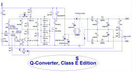

Here is a look at the circuit:
U5 is the master oscillator; R1 determines the OFF time, which should be sligtly smaller than the tank circuit's pseudo-period (~10µs).
The ON time is determined by the current from the feedback transistor, be it alone or part of an optocoupler. Resistors R3 and R4 set limits to that time: it would be unhealthy to allow a zero or infinite ON time.
R3 sets the maximum conduction time (thus the maximum output power). With 27K, this time is the same as the OFF time.
R4 sets the minimum conduction time: it is preferable to have a OFF time slightly smaller than the tank's own period and a finite ON time, to ease the synchronisation between the oscillator and the resonant circuit for light or zero-load conditions, otherwise it could skip a cycle and break into a chaotic mode.
C10 needs to be selected, because the dispersion for the 74HC14 is quite large.
Together, these elements allow a variation of frequency between 50kHz (max load) and 100kHz (no load).
With an optocoupler, the base can be used for a soft-start: the isolated version has a strong surge current at startup, because of the saturation of the CMC and the capacitors to charge.
With the startup, there is no current overshoot at all; it is optional though: if the source can tolerate it, it is not required.
The capacitor C4 is always required, even without additional circuit: phototransistors have a large Miller capacitance, and this interferes with the oscillator
The CMC is connected directly across the main inductor: its inductance is much higher, and does not alter its value.
An optional capacitor is shown: it could be required if the DC resistance of the CMC is similar to that of the inductor, as this would cause a DC current to flow in the CMC.
CMC's have a gapless core, and do not tolerate more than a few tens of mA of DC current.
Here, the resistances ratio is very large, and no capacitor is required.
CMC's aren't ideal as transformers: they generally use a large-µ, dissipative ferrite material causing some additional losses and very sensitive to DC bias.
It doesn't pose a great problem though.
More problematic is the absence of data regarding the transformer operation: you know the inductance, the DC resistance, sometimes the capacitance and maximum voltage but not the V*s product, required to dimension a primary winding (it is determined by the effective core area, the number of turns and the max induction).
With CMC's in the mH/A range though, the product seems to be sufficient to operate in the tens of kHz range without risking saturation.
The rectifiers are always based on doublers: for the non-isolated version this is necessary because single diodes would yield different voltages for the + and - outputs, since the coil is referenced to the +5V.
There is no such problem with the isolated version, but if the DC output currents are unbalanced, it will cause a net magnetization at the secondary, which is not tolerable
The voltage regulation circuit (D9) is rudimentary, but sufficient for the task: it keeps the output voltages within a few hundreds mV of their nominal value, which is OK for the subsequent linear regulator.
If required, the regulation can be made tighter by reducing the resistance level of the adjustment divider (R7, R8).
At some point, the increase in loop gain may cause instabilities, as there is no explicit compensation.
If a really tight and well-compensated regulation is required, the traditional solution of a TL431 as an error amplifier driving the opto should be used, as it allows the loop response to be optimized.
The tracking between the + and - voltages is excellent, even with widely different loads.
The main disadvantage of this scheme is its poor efficiency: around 70% in my example.
The free-wheeling diode and secondary rectifiers impose a 10~15% and 5~7% incompressible penalty from the start, limiting the ultimate efficiency attainable to 80%, even if all the rest is pretty optimal.
My build is 10% lower because of the MOS Rdson, the imperfect (home-made) inductor, the metallized PP cap (a plain foil type would be better), and various other small losses, like the esr of the output caps.
If the circuit is used with a 3.3V supply, the losses caused by the free-wheeling diode will be even higher.
My build is also rather bulky (30x70mm), but this is due to the components, which are 30 years old TH commodities (with the exception of the MOSFet).
With modern SMD components, the size could be more than halved very easily.
With adequate types of CMC's, the circuit can provide many hundreds volt of isolation, making it suitable for use in tube circuits, for elevated heathers, and various floating supplies like bias, or in difficult topologies like circlotron.
Remember that this is functional isolation though, and cannot be used as a safety barrier between mains and user: CMC's are normally not "Y" type components, even if they withstand 250VAC or more between their windings.
Last edited:
The 74HC14 has a supply bypass: R2 C11. In an ideal world, it shouldn't be necessary, but I made the mistake of picking its supply from the positive side of L1/C2, where some perturbations are present.
I should have connected it directly to to C3/C6, but having R2 present has advantages: it allows you to power the oscillator alone, to chose the proper value of C10 without having to worry about misdriving the power section.
Once the capacitor is in place, you can add a second supply on the power side, and increase the voltage progressively, to check if everything works as it should, without risking to fry a component or having to rely on the supply's limitation to mitigate problems.
If the RC cell is not implemented (which could be the case with a sensible layout), it would be a good idea to include a jumper, to separate the power and drive supplies during tests.
The last oscillogram, downstream of the CMC shows a relatively harsh waveform, with a rather violent edge, which is exactly what we want to avoid in a clean supply.
It is possible to soften the edges by connecting a 47 to 100nF across the secondary.
Due to the mode of operation, the impact on the losses is negligible: in fact, for up to 70nF, the losses decrease (very) slightly for unclear reasons.
The straight capacitor connection causes a bit of LF ringing on the flat, mid-part of the waveform, but the amplitude and frequency are benign and no cause to worry.
It would be possible to damp them completely with an appropriate snubber, but it doesn't seem necessary.
I'm enjoying the progress Elvee  . At one time the interest was to dc/dc convert 48V battery feed down to 12V rather than up. I got a non-isolated 2MHz class E to provide regulated 60W output at 83% efficiency using a vintage IRF230. Switching frequency generation and output voltage regulation used an LS629. That frequency (and the topology I used) did need two air-core inductors and 2 small pot-core inductors, although it did turn out pretty small for 60W, and the aim was to use as high a switching frequency as possible (although 2MHz soon wasn't too high for dc/dc).
. At one time the interest was to dc/dc convert 48V battery feed down to 12V rather than up. I got a non-isolated 2MHz class E to provide regulated 60W output at 83% efficiency using a vintage IRF230. Switching frequency generation and output voltage regulation used an LS629. That frequency (and the topology I used) did need two air-core inductors and 2 small pot-core inductors, although it did turn out pretty small for 60W, and the aim was to use as high a switching frequency as possible (although 2MHz soon wasn't too high for dc/dc).With relatively high supply voltages, the effect of the freewheeling diode (if you used one) on the efficiency becomes much less important, and this certainly helps.
For the moment, I have remained in the 50 to 150kHz range, but there is no reason why higher frequencies shouldn't be reachable: with the 74HC14, a five-fold increase is certainly possible, maybe more.
With a 74AC14, a ten to fifteen time increase should be manageable
For the moment, I have remained in the 50 to 150kHz range, but there is no reason why higher frequencies shouldn't be reachable: with the 74HC14, a five-fold increase is certainly possible, maybe more.
With a 74AC14, a ten to fifteen time increase should be manageable
No freewheeling diode - it was a pure class E inverter stage with resonant LC followed by impedance matching stage - Cds of the FET had to be augmented with fixed cap to get resonant zero voltage switching - so quite different from what you are contending with. I'd imagine there are many interesting design loops that could be worked through and that the inductors probably end up dictating frequency range due to core and winding losses, and the transformer seems like a minefield to navigate.
Interesting: if there are no rights or IP issues, you could publish the design on this thread (or a dedicated one), it would certainly be instructive, and spark other ideas, maybe some kind of hybrid?
This scheme can be made to work as a buck converter too: the most obvious method (but not necessarily the best) would be the splitting of the resonant capacitor, to create a capacitive divider.
Such a converter would still be compatible with a low quality isolation transformer (the CMC)
This scheme can be made to work as a buck converter too: the most obvious method (but not necessarily the best) would be the splitting of the resonant capacitor, to create a capacitive divider.
Such a converter would still be compatible with a low quality isolation transformer (the CMC)
- Home
- Amplifiers
- Power Supplies
- Q-conv, SE + Class E edition