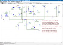
I think that the ripple from power supply is responsible for at least 30% of "transistor sound". In a way to reduce ripple I have invented this push-pull schematic. I have no intentions to patent it (I already have 3 patents and never made any decent money from them). If it is new I proclaim it public domain (with my name attached to it "Podoliak").
The circuit works as follows:
1). the signal from usual rectifier -WITHOUT SMOOTHING CAPACITOR - is splitted into two regular zener-diode voltage regulator.
2). One regulator has zener-diode lifted from ground to collector - thus the bias resistor and zener diode are interchanged in one regulator. At this point the outputs of both linear regulators can be smoothed by capacitors. The voltage of zener diode(s) should be near 50% .. 55% of max amplitude of signal from rectifier.
Thus, one regulator cuts the upper half of a signal, the other - the lower half.
3). The two signals from both regulators are then summed in bipolar transistor (with high max base-emitter current limit).
4). The output can be smoothed by capacitor in a usual way.
There are two basic schematics in this concept:
= one with lower half - feed into collector of summing bipolar;
= another - lower half - feed into the base of summing bipolar.
This schematic:
a). increses the utilization of signal from rectifier.
b). provides smoothing of two near-equal signal by summing them.
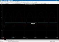
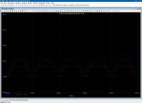
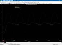
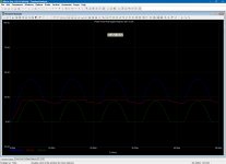
At this point it is just a concept schematic, modelled in MicroCap 11 (9,10) software.
Transient -local pictures show rectifier signal, base of upper transistor, base of lower transistor.
Working title was (like in Hollywood) "push-pull rectifier".
The circuit works as follows:
1). the signal from usual rectifier -WITHOUT SMOOTHING CAPACITOR - is splitted into two regular zener-diode voltage regulator.
2). One regulator has zener-diode lifted from ground to collector - thus the bias resistor and zener diode are interchanged in one regulator. At this point the outputs of both linear regulators can be smoothed by capacitors. The voltage of zener diode(s) should be near 50% .. 55% of max amplitude of signal from rectifier.
Thus, one regulator cuts the upper half of a signal, the other - the lower half.
3). The two signals from both regulators are then summed in bipolar transistor (with high max base-emitter current limit).
4). The output can be smoothed by capacitor in a usual way.
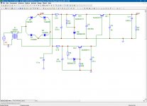
There are two basic schematics in this concept:
= one with lower half - feed into collector of summing bipolar;
= another - lower half - feed into the base of summing bipolar.
This schematic:
a). increses the utilization of signal from rectifier.
b). provides smoothing of two near-equal signal by summing them.
At this point it is just a concept schematic, modelled in MicroCap 11 (9,10) software.
Transient -local pictures show rectifier signal, base of upper transistor, base of lower transistor.
Working title was (like in Hollywood) "push-pull rectifier".
Attachments
-
 Push-Pull-001-2-Schematic.jpg449.4 KB · Views: 387
 -
 Push-Pull-001-2-Transient-Global.jpg310.7 KB · Views: 379
 -
 Push-Pull-001-2-Transient-Local.jpg319.9 KB · Views: 349
 -
 Push-Pull-001-3-Schematic.jpg332.1 KB · Views: 382
 -
 Push-Pull-001-3-Transient-Global.jpg306.8 KB · Views: 357
 -
 Push-Pull-001-3-Transient-Local.jpg327 KB · Views: 185
Last edited:
What might be of interest is to compare this method with a 'normal' method for ripple with the same load and the same input power.
Jan
Jan
We need real measurements so we could compare.Any thoughts?
If you are talking about a 'transistor sound' then it possibly has to be some comparison of real audio-systems. Possibly with a persons who can hear a difference.
This circuit connects two emitter followers (transistors Q1 & Q3) in series, between the rectifiers and the output. Some people, including me, would prefer to use those two emitter followers to implement two individual capacitance multiplier circuits, connected in series. The advantage is low "dropout" voltage (Voutput - VrectifierPeak).
Capacitance multiplier has high output impedance, that is it's main disadvantage, limiting it to preamp stages only.This circuit connects two emitter followers (transistors Q1 & Q3) in series, between the rectifiers and the output. Some people, including me, would prefer to use those two emitter followers to implement two individual capacitance multiplier circuits, connected in series. The advantage is low "dropout" voltage (Voutput - VrectifierPeak).
Instead this invention has no such limitation (seems to be) and can be used even with output full power stage.
And yes, capacitance multiplier can be used WITH this schematic, in addition, before summ-ating last transistor, with accordingly, lowered ripple.
The output of the bridge rectifier drops to zero twice in a cycle.Where will you get the energy to fill that gap 😕
Mona
Mona
The usual in any rectifier way: from (smoothing) capacitors, C4, C5, C7(C9).The output of the bridge rectifier drops to zero twice in a cycle.Where will you get the energy to fill that gap 😕
Mona
C7 (C9) in this schematic is small 5.0 uF - just to show how the method works. In reality C7 (C9) should be 100.0+ uF for sure.
Add: the advantage of this method is that
= in prior art "rectifier + zener-regulator" the power signal is collected in capacitor immediately after rectifier, then suppressed by trainsistor+zener diode schematic.
= instead, in this invention the power signal first has been CUT (to it's 50...70% of max amplitude, RMS value) by transistor+zener diode schematic, and only after that the power signal is collected (smoothed) by two capacitors; then the two cut-and-smoothed signals are summed by output bipolar transistor.
Last edited:
Capacitance multiplier has high output impedance, that is it's main disadvantage, .
Your emitter followers have exactly the same output impedance.
Jan
Sorry, no.Your emitter followers have exactly the same output impedance.
Jan
There is a huge difference:
There is NO capacitor in low part (Cap shunting the resistor or zener diode, as in cap-multiplier) on each sleeve.
They are simply two plain regular linear regulator with zener diode. No difference to usual design, and thus have low output impedance.
The one (sleeve) cuts lower part of sine wave - as ANY usual linear regulator. Absolutely no difference with well-knowing schematics.
The other one cuts the UPPER part of sine wave - that is the difference to usual design.
- Home
- Amplifiers
- Power Supplies
- Push-pull ripple rejector (by Podoliak)