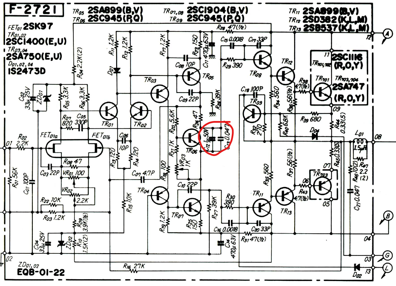
Wondering what the purpose/function of C12 and C13 is in this schematic?
I'm assuming C13 is added because C12 was less than ideal?
(It's from a Sansui AU-717 driver board).
Anybody who can explain?

I'm assuming C13 is added because C12 was less than ideal?
(It's from a Sansui AU-717 driver board).
Anybody who can explain?
Looks like it is an electrolytic bypassed with a film cap. It is part of a bias spreader circuit using TR06 along with vr03 for bias adjust. Might be worth replacing c12 and just testing c13.
The purpose is to not allow a change for ac and allow some dc value to set output bias.
The purpose is to not allow a change for ac and allow some dc value to set output bias.
C13 improve the AC short at high frequencies of the CE junction, since C12 being an electrolytIc has some serial built in inductance.