Eva,
I have an Adobe writer on my work laptop, but try looking up cutepdf.
I lets you generate PDFs from any windows program
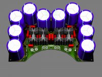
Any comments on the schematics?
\Jens
I have an Adobe writer on my work laptop, but try looking up cutepdf.
I lets you generate PDFs from any windows program
Any comments on the schematics?
\Jens
Hi Jens,
how about leaving a resistor gap on each cap (C1, 2, 10, 11 etc) to allow RC snubbers across the rectifiers. Either link across or add R to suit.
I would raise the value of the cap discharge resistors. 10k to 20k would suffice.
I am not a believer of fuse in the supply to the rectifier. Provide a mains primary fuse and optionally secondary fuses after the smoothing caps.
A fuse before the caps has to survive a very big charging pulse and would need to be T rated as well as large value (I'm not sure your proposed T5A will survive). Then fuses in this early location are of little protection value when serious faults develop down stream.
Try adding a 100n across the bridge + to - and ~ to ~ but at the rectifier location to give best attenuation of high frequency spikes before track inductance reduces their effect.
The capacitor that (by experimentation with real components) I have found to be optimum in order to supress the sharp turn-off spike of conventional diode bridges, without causing more ringing than it supresses, is just a single 22nF across both AC terminals of each bridge (as close as possible). No more capacitors are required, altough a RC network in paralell with that 22nF capacitor may help to damp transformer winding resonance (values here are highly transformer-dependent, the range for big EIs is probably 100nF and 47ohm).
MUR diodes are probably going to require smaller capacitances because the recovery times are an order of magnitude lower.
EDIT: Have you considered placing +Vcc and -Vss outputs near the ground output to reduce wiring inductance?
MUR diodes are probably going to require smaller capacitances because the recovery times are an order of magnitude lower.
EDIT: Have you considered placing +Vcc and -Vss outputs near the ground output to reduce wiring inductance?
Eva,
So you think that a snobber on the AC connection is all that I need to worrie about?
EDIT: YES, but I plan to twist the supply wires to the amp with 2-3 gnd wires
\Jens
So you think that a snobber on the AC connection is all that I need to worrie about?
EDIT: YES, but I plan to twist the supply wires to the amp with 2-3 gnd wires
\Jens
The resistor that I mentioned is subject to negligible dissipation, as it has to damp a couple of several-thousand Khz oscillations with less than a dozen volts amplitude only 100 times per second. A 0.25W one is enough (even a 0.125W SMD one would do).
The only capacitors that I tried (both for the direct C and the additional RC) were small square plastic films (plastic case, probably MKT). I couldn't compare to ceramics because I didn't have 22nF and the 100nF ones that I had were multilayer and rated at 50V only.
My whole experiment is described here:
http://www.diyaudio.com/forums/showthread.php?s=&threadid=66542&perpage=10&pagenumber=7
It has plenty of oscilloscope captures showing what happens with different capacitor values.
Thanks Eva!
I will make room for a snobber on the AC inputs.
I will update the schematics tonight and post the final version
\Jens
I will make room for a snobber on the AC inputs.
I will update the schematics tonight and post the final version
\Jens
Eva,
What is your experience with combining film, electrolytic and ceramic caps in parallel to get a wide band low impedance for the noise generated in the rectifier stage?
I’m thinking of using 1210 100V 2.2µF types right at the output terminals and at the DC pins of the diodes.
Thanks for any input
\Jens
My experience in SMPS is that films parelelled with electrolytics resonate, and the same happens with films paralelled with ceramics. I have no data about ceramics paralelled with electrolytics.
However, this is a hard question because capacitor ESR and PCB ohmic resistance will damp the resonance, while PCB inductance and component lead inductance will worsen it dramatically.
Do you feel like building a small pulse-generator and trying it? I'm currently busy with some urgent projects.
Also, I have not yet found any evidence of electrolytic capacitors of any size between 1uF and 10.000uF becoming inductive below at least 1Mhz. Wiring inductance (and PCB layout) will have a much greater impact on PSU inductance, so there is no point in trying to keep PSU non-inductive above 1Mhz anyway.
However, considering that most people is more focused on popular wisdom about paralelling capacitors rather than on the electronic phenomena behind it, you should leave plenty of room for exotic capacitors if you want your boards to become popular (they enjoy knowing that the purple-and-yellow-striped-gate capacitors are there 😀 ).
I have a network analyzer at work, so I can sweep whatever configuration I can imagine.
I might look into making some sweeps of the different parts I'm looking at.
I have been using ceramics at work for my different DC/DC converters and know that the ESR + ESL are very very low....
A lot will depend on the PCB layout, so short returnpaths + low inductance (gndplane) is a must and DC resistance must be lowered to a minimum.
I will problably do a prototype board with room for different parts and try out different configurations.
I'll keep you posted
\Jens
- Status
- Not open for further replies.
- Home
- Amplifiers
- Power Supplies
- PSU for my Leach AMP