Hi all
A workmate of mine has asked me to repair his Proton D940 receiver (blown output). Has anyone got a schematic diagram of this one ?
Regards
Charles
A workmate of mine has asked me to repair his Proton D940 receiver (blown output). Has anyone got a schematic diagram of this one ?
Regards
Charles
I'm also looking for a schematic for a D940, pretty shure my output transistors are shot too. I just picked this reciever up, would have payed WAY less if the seller indicated it was fried😡 . When the unit is powered up with a source connected (CD player) the overload protection clicks immediately (no speakers attatched). The crazy...and I mean crazy thing is if you turn the volume up enough you can actually hear music eminating from the bread board (shakes head)!!! The output transistors do not seem to get very hot, there are a total of 8 of them . I'm going to put he VOM on them and see what I get for resistance, any advice would be greatly appreciated.
Hi Guys,
I put in a request at ShareFx for you. Let's hope someone out there can help you out. I'll try to post if I can get it.
-Chris
Edit: Charles, do you still need these?
I put in a request at ShareFx for you. Let's hope someone out there can help you out. I'll try to post if I can get it.
-Chris
Edit: Charles, do you still need these?

 , I could use all the help I can get.
I'm pretty sure Proton and NAD are the same thing. Try and figure out what the equivalent NAD model is to yours - since NAD's are more common you may have more luck in getting the schematic that way.
Yep, I have been looking at a few NAD schematics and nude pics folks have posted on the net but so far I see the same weird heat sink but totaly different output transistors and breadboard. The proton uses SanKen A1186,A1386A, A1386 and C3519A, C2837, C3519. Things are not looking up for the Proton, board is slightly brown over by the safety relays and power transistors (all are HOT) .Still wondering how my breadboard is making music?!
.Still wondering how my breadboard is making music?!I have a Proton AM-300 that looks as if it got the same power amp stage as D940, and I have a copy of the ORIGINAL service manual of it too.
If you guys still needs it, please let me know, I'll scan the pages of the service manual's circuit and post it.
However, I'd really be happy if someone could post a high res pic of both the overhead shot and underside shot of D940, as I'm thinking about getting one myself 😛
However, if D940 is what I think it is, then you will have to match the output transistor VERY CLOSELY, since they do not have any resistors connected to the emitter of the transistor, just straight wire. But you only need two pairs to be matched, the other two pair are for DPD power boost, and they don't need to be matched at all, just make sure they work well, that's all 😛
Forgot to mention, from my own AM-300, it seems as if the really good engineer only designed the REALLY hard part of the amp, the power amp stage. The rest seems to be left to junior engineers...
The result is fairly bad power supply attention on the pre, and rather lousy wiring performance for the speaker output.
#1. The pre/tone control section can really benefit from some power rail bypassing, and the stupid coupling cap can be removed for much better clarity. As for me, I bypassed the entire tone control section, which I don't really use at all anyways.
Please do note that it seems to be a 2.5V potential at the input of the power stage, the coupling between pre and power stage must be kept.
#2. The speaker wiring on mine is a disaster, not only the wiring is too long on lousy wires, it went through some rather lousy mechanical switches. Just tore it out, replace the speaker binding post, and use short, direct wires had made most difference I have ever heard while modding this amp. None of the resistor mod, capacitor bypass, better coupling caps, and the like can even hold a candle to this.
Ah well, that's all I can say now, I'll go and do some scanning when I get home.
Hi Maniac,
Would you be willing to email it directly in higher resolution? My address is bhomester at gmail dot com. Let the other guys post their email addresses as well so you only have to send it out once to all parties. Easier on you and I can wait.
-Chris
That would be very kind of you! However, the attachment size is very small (100 KB).If you guys still needs it, please let me know, I'll scan the pages of the service manual's circuit and post it.
Would you be willing to email it directly in higher resolution? My address is bhomester at gmail dot com. Let the other guys post their email addresses as well so you only have to send it out once to all parties. Easier on you and I can wait.
-Chris
anatech said:Hi Maniac,
That would be very kind of you! However, the attachment size is very small (100 KB).
Would you be willing to email it directly in higher resolution? My address is bhomester at gmail dot com. Let the other guys post their email addresses as well so you only have to send it out once to all parties. Easier on you and I can wait.
-Chris
Well, I just dug out some partial scans that I made of the amp, this following pic is of the power amp stage. This pic represents both channel of the amp, and all parts number/value should be there with the parts, if a part does not have it indicated, please check the corresponding part in the other channel.
An externally hosted image should be here but it was not working when we last tested it.
Well, people, here it is...
Let me know if you find something funny in the scan. this is a fold out page, so there's some gap in the middle, but that should be a snap for anyone to fill in the blanks in their head. 😛
An externally hosted image should be here but it was not working when we last tested it.
Let me know if you find something funny in the scan. this is a fold out page, so there's some gap in the middle, but that should be a snap for anyone to fill in the blanks in their head. 😛
Many thanks Maniac!! I'd be happy to take a few pics of the D940, though the upper portion is pretty cluttered. Since there are a total of 8 output transisitors I figuured one set must be devoted entirely to DPD.
S.Spielbergo said:Many thanks Maniac!! I'd be happy to take a few pics of the D940, though the upper portion is pretty cluttered. Since there are a total of 8 output transisitors I figuured one set must be devoted entirely to DPD.
if you can show me a pic of the bottom, I should be able to tell you.
The DPD transistors are usually grouped in the middle where two pairs of NPN and two pairs of PNP are grouped together. the actual transistor that does the ampilification is the PNP/NPN pair with a temp compensation transistor there. As for those, they are usually grouped on the two side of the heatsink, so that each channel gets spaced as far apart as possible from the other channel.
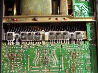
Here is a pic of the underside of the amp board. The topside doesn't reveal much with the tuner in place unfortunately. The really hot transistors are Hitachi B649A's (4 of them), looks like they are going to be hard to find, the c3519A/a1386A are also tough to find though MCM electronics lists sa1294/c3263 as replacements.
Attachments
S.Spielbergo said:Here is a pic of the underside of the amp board. The topside doesn't reveal much with the tuner in place unfortunately. The really hot transistors are Hitachi B649A's (4 of them), looks like they are going to be hard to find, the c3519A/a1386A are also tough to find though MCM electronics lists sa1294/c3263 as replacements.
the 4 transistor in the center are for DPD and are not usually turned on at all. The amp should still work at low power mode if those 4 are removed. The trio on either side of the heatsink are for actual amplification.
Personally speaking, if you found the transistor for amplification was damage/dead, and could not find a proper replacement. It should be possible to take transistor from DPD section and use if for amplification.
HOWEVER... I have not tested if there are any difference between the transistor for DPD and transistor for amplification. It could very well be that the transistor for amplification was cherry picked and whatever leftover was used for DPD.
My idea would be that if you have at least one good channel, take the transistor off and measure the HFE of both PNP and NPN. so that you get an idea of how good the pair match, and their average HFE level. Then stick the pair back to where they belong, and measure the ones from the DPD circuit, if they are similarly matched at similar HFE level.... Well... 😀
If the above worked or if you blown DPD transistors (now sure how's that gonna happen), DPD transistors should not be hard to replace. Just matching pinout and something close in HFE and current/voltage rating would do. It is not something that is working all the time, and even when it is working, it is just acting as a switch anyways.
Thanks for some of the insight but I'm a little fuzzy on which transistors are used for what. Are the 4 centermost transistors used for DPD, while the last four flanking the outside are used for normal amplification? I know my picture isn't super detailed so what I have for transistors from left to right is A1386,C3519,C2837,C2837,A1186,A1186,A1386A,C3519A.
I'm a little confused as to why Proton would use slightly different chip sets from left to right channels (A1386/C3519 vs A1386A/C3519A). I unfortunately have NO working channels, with preamp jumpers removed I tested each channel but the unit went into protection just as soon as the volume knob is touched (no source connected).So there is a short downstream of the protection relay, but since it shorts only the volume knob is cracked I assumed it was in the output stage (preamp section works fine).
I'm a little confused as to why Proton would use slightly different chip sets from left to right channels (A1386/C3519 vs A1386A/C3519A). I unfortunately have NO working channels, with preamp jumpers removed I tested each channel but the unit went into protection just as soon as the volume knob is touched (no source connected).So there is a short downstream of the protection relay, but since it shorts only the volume knob is cracked I assumed it was in the output stage (preamp section works fine).
S.Spielbergo said:Thanks for some of the insight but I'm a little fuzzy on which transistors are used for what. Are the 4 centermost transistors used for DPD, while the last four flanking the outside are used for normal amplification? I know my picture isn't super detailed so what I have for transistors from left to right is A1386,C3519,C2837,C2837,A1186,A1186,A1386A,C3519A.
I'm a little confused as to why Proton would use slightly different chip sets from left to right channels (A1386/C3519 vs A1386A/C3519A). I unfortunately have NO working channels, with preamp jumpers removed I tested each channel but the unit went into protection just as soon as the volume knob is touched (no source connected).So there is a short downstream of the protection relay, but since it shorts only the volume knob is cracked I assumed it was in the output stage (preamp section works fine).
C2837,C2837,A1186,A1186 is for DPD.
This is kinda weird. As you can see in the schematics, AM-300 have no such type of protection. I wonder if it is possible to maybe solder a couple wires to the input of the relay and measure it. See if there's something funny that the power stage is sending out.
IMHO, it is normal for power stage to have a little bit of DC components, if it is below 0.5V then I'm not worried at all. 😛
- Status
- Not open for further replies.
- Home
- Amplifiers
- Solid State
- Proton D940 schematic ?