Hey all, I've got a reasonably complex amplifier I'm about to build, and I went and purchased a bunch of radioshack protoboards . Am I OK to use these as long as I don't put any enormous current thru them? The heaters and the output stage current won't go thru the board, its mainly for the feedback loops and biasing, but it would be incredibly convenient. My B+ will be 200V.
Thanks all
Thanks all
I think you will do just fine with those boards.
I have a couple of those myself.
With islands of 3 point per each.
I have a couple of those myself.
With islands of 3 point per each.
I think you will do just fine with those boards.
I have a couple of those myself.
With islands of 3 point per each.
Thanks! Have you used them at tube voltages?
Those protoboards are intended for use with low voltage solid state circuitry. The space between copper islands is about 0.015 inch, not enough to stand off high voltage between the copper islands. I would not use these boards beyond 30 volts or so (+/-15V).
The other issue is that the board contains long parallel pieces of copper closely spaced so there will be a fair amount of capacitance between adjacent conductors. You mentioned feedback loop components and that might be a bad place in the circuit for stray capacitance to crop up.
I would look for a proto board with no copper on it, but drilled with a grid of holes on 0.1" centers like to board you referenced. Then just place the components and wire point to point with hookup wire.
There are tube protoboard that have tube socket foot print and better spacing. Why not get some of those. Break down voltage of air is ~3000V/mm. These (0.38mm) are cutting it close.
I have been using these. I leave an extra space or two around the plate pins and anything connected to B+ and have had no issues up to 400 V. Uxcell a14061100ux0395 10 Piece DIY Universal Single Sided PCB Printed Circuit Board 9 cm x 15 cm, 3.54" Width, 5.91" Length: Amazon.com: Industrial & Scientific
I have been using these. I leave an extra space or two around the plate pins and anything connected to B+ and have had no issues up to 400 V
Uxcell a14061100ux0395 10 Piece DIY Universal Single Sided PCB Printed Circuit Board 9 cm x 15 cm, 3.54" Width, 5.91" Length: Amazon.com: Industrial & Scientific
So you think if I leave an extra row between anything that has a potential difference of 100V+ I should be ok? The only big voltage drops are B+ to ground and then across the plate so I think I'll be alright. This will make construction much easier as I can use 2 of these boards but would need around 8 terminal strips otherwise...
Thanks for the response
The rating on some is just 48V.
This may be a "cover our butt" conservative rating. It is reckless to have "dangerous" voltages on exposed part leads, and 48V is one common "max safe" voltage. So that is what the protoboard specs tell you.
As George proves, they don't explode at 49V adjacent, and you can use alternate rows, At Your Own Risk.
If you're concerned about arcing between pads, you can always remove the adjacent pads with a drill bit. This process is a bit easier on the boards that just have holes and individual pads, but will work on the board you show as well.
If all you plan to put on the board is feedback and biasing, you might be able to have the voltages on the board be pretty low and have the high-voltage connections go off the board through a component.
I use the Saturn PCB Toolkit to figure out the appropriate spacing between traces and pads.
Tom
If all you plan to put on the board is feedback and biasing, you might be able to have the voltages on the board be pretty low and have the high-voltage connections go off the board through a component.
I use the Saturn PCB Toolkit to figure out the appropriate spacing between traces and pads.
Tom
On perfboard with one hole per pad, it is easy to overheat the pads with a soldering iron and scrape them off. I always scrape off at least three rows between anything connected to the 230 V AC mains and anything that's supposed to be galvanically insulated from the mains to ensure that the creapage distance is more than 6 mm. For tube circuits, I prefer the perfboard with no copper at all, so I don't have to worry about what to scrape off.
Last edited:
Oh, that's true. I forgot about the heat-and-scrape method. If the board is thru-plated, you can always drill out the plating. Then heat-and-scrape.
Tom
Tom
I have been using these. I leave an extra space or two around the plate pins and anything connected to B+ and have had no issues up to 400 V
Uxcell a14061100ux0395 10 Piece DIY Universal Single Sided PCB Printed Circuit Board 9 cm x 15 cm, 3.54" Width, 5.91" Length: Amazon.com: Industrial & Scientific
I use ones similar to these as well. I like the kind with round eyelets that are on one side only. If you are really paranoid, it is often possible to strip off some eyelets with an exacto type knife, but I rarely find that necessary.
The best boards are epoxy. I had a nice big one from my local supply that I cut down to more manageable sizes. Some experimenter boards on that popular auction site claim they are epoxy, but are only perhaps very thinly coated epoxy (beware).
On perfboard with one hole per pad, it is easy to overheat the pads with a soldering iron and scrape them off. I always scrape off at least three rows between anything connected to the 230 V AC mains and anything that's supposed to be galvanically insulated from the mains to ensure that the creapage distance is more than 6 mm. For tube circuits, I prefer the perfboard with no copper at all, so I don't have to worry about what to scrape off.
excellent practice. you are more paranoid than me. 😀
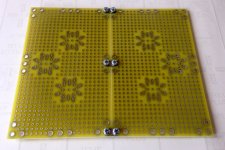
Prototyping board listed by initial thread poster poorly suits tube circuits. There are several variants of prototyping boards on eBay made in China. I tried them and found 1.5mm FR4 is too rigid, there is a considerable mechanical force when one need to pull / take out tube from socket. Additionally, placeholders for sockets aren't universal as they should be.
So I ended with my own, made with 2mm FR4 with universal tube sockets for 7, 8 and 9 pin variants.
So I ended with my own, made with 2mm FR4 with universal tube sockets for 7, 8 and 9 pin variants.
Attachments
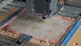
Last PCB prototyping board (similar to the one in my previous post), yet larger (250 x 165mm / 9.84" x 6.49), 5mm pitch, 6 placeholders for tube sockets, octagonal pads for max copper area and max space in between at the same time, milled (depth = 0.2mm) on my DIY CNC router.
Attachments
Since you make your own; you could also incorporate bus "traces" into your boards. Like a ground bus, and Vb bus with provisions for RC filering etc. and leave the rest of board space for the circuit itself.
Since you make your own; you could also incorporate bus "traces" into your boards. Like a ground bus, and Vb bus with provisions for RC filering etc. and leave the rest of board space for the circuit itself.
With the last (largest one) I actually did this.
Can't understand how this idea was so late in my mind.
- Status
- Not open for further replies.
- Home
- Amplifiers
- Tubes / Valves
- Protoboards OK?