
Going back to the OP question, the diodes have nothing to do with the capacitor failure, but are a sensible move to prevent one of the supplies reversing and various parts latching up, especially regulators. I always used Schottkys for this when I had latching trouble
The current source is fine, but something else is very wrong.
There are many possible causes. If you could measure and report some node voltages throughout the amplifier circuit, maybe we can narrow it down.
I'll add some specifics to Marcel's recommendations.
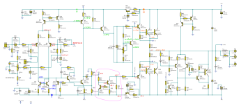
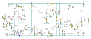
With respect to ground, I suggest measuring:
Left Output
Base of Q5
Base of Q6
C6
Collector of Q3
With respect to +Rail2:
B,C,E of Q4
Emitter of Q33
B,C,E of Q12
With respect to +Rail:
B,E of Q1
E of Q13
Left Out
B,E of Q15
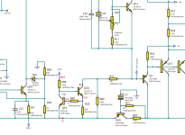
I have a very skeptical perspective of all the circuitry between Q29 and Q18/Q18, perhaps because I don't understand its purpose or how it can bias reliably. Does any of your documentation discuss this circuitry? (You didn't mention the model number.) In any case, I advise disabling this circuit until the rest of the amp is debugged, just to remove it from suspicion. There may be a switch controlling "XD On/Off" that would disable. Alternately, you can install a temporary short across R58 to disable.
Thanks!
The model is Cambridge A. 840.
XD (on/off) is their version of class A.
I power it independently, with an external transformer,
R58 is shorted,
are also disconnected: +- Drive protect, +-Re, the connection of the output with DC offset Detect and Clip detection
Here are the numbers:
With respect to ground:
Left Output - 30.5V
Base of Q5 - 153mV
Base of Q6 - 14.72V
C6 - 14.44V
Collector of Q3 - 1.232V
With respect to +Rail2:
Q4 B - -1.181V, C - -1.131V, E - -1.131V
Emitter of Q33 - -1.77V
Q12 B - -3.722V, C - -1.793V, E - -4.345V
With respect to +Rail:
Q1 B - -3.38V, E - -4.03V
Q13 B - -4V, E - 4.6V
Left Out - -4.6V
Q15 B - -5.23V, E - -4.7V
The voltages vary slightly, the radiator heats up a bit.
If it's more convenient, I can put them to the scheme.
Regards!
Last edited:
I should have also ask for measurements to show bias on transactions Q7 through Q11, all these with respect to -RAIL2. Your suggestion of noting voltages on schematic sounds ideal. Thanks!
4AM here, so I may not be back for awhile. 😉
4AM here, so I may not be back for awhile. 😉
If this is a stereo amp or a second mono existing, why don't you compare working and defective side, write down values and then change the blown part?
Did you already change Q 34,35? Sometimes the best thing to do, is to change some basic parts that seem to act funny.
It is not worth much to understand the last bit of the construction, if the aim is a repaired amp.
Did you already change Q 34,35? Sometimes the best thing to do, is to change some basic parts that seem to act funny.
It is not worth much to understand the last bit of the construction, if the aim is a repaired amp.
Has Q4 become a short circuit?
(The circuit around Q9, Q10, R9, D10 doesn't manage to pull down Q10's collector, but I think that is due to their current limiting feature.)
Once you have everything biasing normally again, please replace the input transistors. Q6 is emitter-base avalanching, which worsens its 1/f noise, among other things.
Nice work. By “Q7 through Q11” I meant Q7,Q8,Q9,Q10,Q11. Sorry I wasn’t more clear.
I’m going to guess Q9 emitter is about 4.3V and Q10 emitter is about 3.7 but collector is near the positive rail. Make sure R9 is still good, but likely Q10 has failed.
Marcel has made a good point about Q6. It might be a good idea to add some clamp diodes to protect these transistors.
Q4 could have shorted, but if so, Q10 should be quite warm; probably cool if it’s open.
Last edited:
R9 is good
I disolder Q10, the tester showed that it was ok.
Q4 it's also ok
I disolder Q10, the tester showed that it was ok.
Q4 it's also ok
Attachments
Last edited:
My personal preference is powered troubleshooting and I try to avoid removing components until I've zeroed in on a suspect. I'm going to attempt a "stream of concisiousness" narrative to show how I troubleshoot. Which is not to say that I'm that great at it...
With 3.79V across R9, there should be 8mA flowing in Q10. There's about 33V across Q10 collector to emitter, so about 0.26W. That should be enough to make Q10 toasty. Does it feel warm? I'd probe directly on the leads of R9 to confirm 3.79V makes it to the body of the resistor.
Assuming Q10 is warm, then the question becomes where is that 8mA flowing? 1.131V across R3 is 7.5mA, so that must be where the the current is going. Maybe Marcel's "Has Q4 become a short circuit?" is spot on! The voltage at collector and emitter is identical; with power off, does Q4 C-E measure as a short in both directions? Q4 base-emitter also looks very odd. I think Marcel has nailed it.
Both transistors Q4 and Q10 are still removed. The tester shows they are fine.
I don't have the exact ones, but I will look for other similar ones for a sample, because my Chinese tester could be wrong.
I don't have the exact ones, but I will look for other similar ones for a sample, because my Chinese tester could be wrong.
If Q4 and Q10 are still absent, let's take advantage and measure with respect to +Rail2: emitter of Q33 and base of Q1.
If the Q4 emitter is only a a volt or two below +Rail2 and the base of Q1 is only slightly lower than Q4 emitter, that sounds reasonable. If that is the case, let's next test the output stage with out any load.
R88 should pull the output stage to near the the positive rail.
Next, tack a 10K resistor to the base od Q33 and ground the other end of the resistor. The output voltage should droop to just a few volts above ground. (The 10K is an expendable current limit resistor.)
Next, remove the same resistor from ground and connect it to the negative rail. Output voltage should move to about 80% of the positive rail, i.e. about 90% of difference between negative and positive rails.
Maybe we'll learn something from these experiments.
I replaced them with 2SD669/2SB649 and everything fell into place. I had already soldered them before I saw your last post.
The offset is 1.1mV and it sounds good.
Can I leave these or search 2SC2911/2SA1209
The offset is 1.1mV and it sounds good.
Can I leave these or search 2SC2911/2SA1209
I have to run errands, so I will check upon return. I'm betting they will be fine.
Great work! 😎
Great work! 😎
I didn't notice any noises, but I only tested for a short time. I will continue tomorrow in more detail.
Regards!
Regards!
Your substitutes look ok to me. I'm convinced Q4 was the culprit, and Q10 likely OK, as it measures well in-circuit once data taken re the negative rail. But since it's been changed, I see no need to undo.
Hi guys,
These days I don't have any free time to put the amp together, but I will someday 🙂
I want to thank everyone who wrote in the thread and especially BSST. I couldn't have done it without your help. Thanks! 🙏
Marcel, what do you recommend Q5 and Q6 be replaced with?
These days I don't have any free time to put the amp together, but I will someday 🙂
I want to thank everyone who wrote in the thread and especially BSST. I couldn't have done it without your help. Thanks! 🙏
Marcel, what do you recommend Q5 and Q6 be replaced with?
- Home
- Amplifiers
- Solid State
- Protection diodes in the power supply