I think DUG's board pretty much fits the bill. It has every possible feature if I am not mistaken. Even the pin 17 isolated AVcc option is there, as well as soft start no pop. I have a couple, just need time to solder the parts. 🙂
I think maybe ALD wants someone in China or Taiwain to make the equivalent of this board and sell it for $25 fully populated 🙂
I think maybe ALD wants someone in China or Taiwain to make the equivalent of this board and sell it for $25 fully populated 🙂
Last edited:
Frequency change not an option on DUG-1 or DUG-2.
Might be able to make a limited number with that option next year. (4 or 8)
🙂
Might be able to make a limited number with that option next year. (4 or 8)
🙂
I'll bang out and sell a PCB, however you'll be putting parts on it yourself.
Yes please! 🙂
I'll bang one out when I'm done with the cAMP design.Yes please! 🙂
Any thoughts on mechanical design? Should I build an "embedded" board with terminal blocks for everything like the cAMP design, or something ready to drop into an enclosure with RCA's, a DC barrel connector, an enable switch, power LED, etc?
""I think DUG's board pretty much fits the bill..."
Errr, check this exact thread.
"I think maybe ALD wants someone in China or Taiwain to make the equivalent of this board and sell it for $25 fully populated 🙂
No, check my critique again. What it looks like is that I want the EVM with a more advance circuit around the other functions ...
Cheers,
Jeff
PS The Weiner is the one to watch for ...
Last edited:
I made some suggestions in the DUG thread but I guess they are better suited here:
1. Do the PSU cap change (page 1) ! I suggest putting the cap holes onto the chip legs. That way you could put the caps over or under the pcb. It will have amazing results on base control and noise floor!
2. Use smaller heat sink! A well designed board gives a super cool chip and chokes. Or use a higher heatsink, or twist it 90 degrees and glue it on! I have done this several times on my boards.
3 Would it be possible to put the bootstrap caps underneath using tinned up via's?
That way they can be super close to the chip and the RC filter can be omitted. Chokes can also be closer to the chip this way.
4. Use film smd caps. They sound supurb!! If the board is getting too large this step could be skipped. But two 100nF film smds as bootstap really do wonders for avoiding sound compression at high levels and makes the amp more stable when maxed out at high voltage!
5. Perhaps use a little better inductors than the super cheap ones? Even barerly better chokes sounds noticable better!
These changes together with the variable frequency option will differentiate this board from all the other pcbs out there, and I think the sound will amaze people even with modded boards!
I'll bang one out when I'm done with the cAMP design.
Any thoughts on mechanical design? Should I build an "embedded" board with terminal blocks for everything like the cAMP design, or something ready to drop into an enclosure with RCA's, a DC barrel connector, an enable switch, power LED, etc?
I am interested in embedded, but the more I read, the more I think I will do my own PCB with 4 channels out, an integrated LiPo charger (Max17005B is leading candidate as it also manage operation from AC), and a battery holder. I will leverage the work done here when I get to it. In the meantime I think DUG's boards and maybe a cAMP will give me plenty to play with.
That all changes if you would consider a 4 channel board with a sigmaDSP for an active crossover. ...
Took a few hours and banged out my take on a 'proper' TPA PCB.

Size is 96mm W, 50mm H. Yeah, the silkscreen's half wrong, I'm not finished yet 🙂
I gave up trying to find a catalog heatsink that would fit the TPA3116 and clear nearby decoupling, and threw the TPA3118 on there instead. The 3118 is only rated for 8 ohm loads in the datasheet, but it uses the same die as the TPA3116 and has a comparable Rjc - and I guarantee the ground plane heatsinking done here works better than the tiny aluminum heatsinks you find on half the eBay TPA3116 cards out there. There's 7 inches of largely unbroken ground plane on the bottom layer, and lots of vias connecting top/bottom layers directly under the TPA.
Input uses film coupling caps, 5mm lead spacing/7.5mm square, typical part would probably be 2.2uF/50V. Spots are provided to put down 10K input resistors between +/-, and a 100 ohm resistor from - to ground for unbalanced input, I might futz with this some more.
Inductors are ICE Components 1D14A, caps for the output filter are 0.68uF/100V film. I'm not using diodes to clamp the post-filter output, thought being if you're pushing the output close to clipping and the output filter is peaking into your speaker load, you could end up with unwanted conduction. Using 100V caps should hopefully keep things from catching on fire with no output load - if not, hole sizes for the film caps are generous so they should be easy to change if they burn up 🙂
5 decoupling cap locations are provided per TPA channel - two 0603 caps, a 1210 cap, and two 10mm diameter caps. An example configuration providing low Z over a wide bandwidth could include a 1000pF NPO, 0.1uF/50V X7R, 4.7uF/50V X7R, a 100uF/35V polymer and a 470uF/35V wet electrolytic. Bootstrap caps (0603 X7R's) are placed tight against the TPA. Immediately next to them are locations for OUTxx snubbers, aka "bootstrap snubbers", with a short return path back to the TPA.
A 4-position DIP switch is provided for adjusting switching frequency and selecting BD/1SPW mode. Gain is set with a pair of 0805 resistors. PLIMIT is currently tied to GVDD, I've contemplated stuffing a pot on there to allow manually setting it like the TI evaluation board provides though I dunno if anyone will use the feature.
I'm using an ATTiny13A microcontroller to provide popless power-on/off and fault handling - originally I had a dual comparator and several discretes handling power sequencing, but decided this was easier. There's a couple pins provided on the input terminal block (/EN and ground) - shorting these two pins turns on the amp, leaving these open turns the amp off with a standby current of ~50uA dominated by the TPA itself, handy for battery powered apps.
Terminal blocks are nice Phoenix rising cage ones that can take 12AWG to 28AWG, and handle 16 amps or something ridiculous.
All parts required to build the card can be ordered from Mouser.
So yeah, probably a bit overengineered compared to everything else out there, it'll be definitely more expensive to build compared to an eBay special, but it should outperform them and allow more customization.
Any change suggestions, thoughts, criticisms, etc... are welcome.
Strong Work Gmarsh ! +1 for U 🙂 Luving the 8-bit too.
The Vias to transfer the switching nodes to L1 & L4... Anyway to lose them ??
All the Vias under the 3118 might be hell to solder.
Dwight
The Vias to transfer the switching nodes to L1 & L4... Anyway to lose them ??
All the Vias under the 3118 might be hell to solder.
Dwight
Very nice board ! It seems the Wiener has arrived. Prepare for a large Group Buy please 😉
Last edited:
May you provide your dual comparator design here? What about switching frequency coupling into PVCC due to having the traces under the inductors? Beside this, nice design, just two thoughts:
You might want rotate the last caps by 180 to have a common GND point for them both (by channel).
The path from PVCC to the first MLCC could/should be narowed at the point/pin of the TH-caps, so that current must flow through that pins, not beside.
You might want rotate the last caps by 180 to have a common GND point for them both (by channel).
The path from PVCC to the first MLCC could/should be narowed at the point/pin of the TH-caps, so that current must flow through that pins, not beside.
Oh, and the Gain-resistors can be recalculated to have them selected via 3 0R jumpers. I did this for my TPA3132D2 boards, so gain setting is just a matter of a solderbridge.
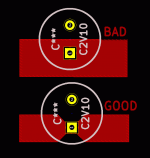
BTW. C21/22 are not in the direct current path, I'd redesign the path.
Regards
BTW. C21/22 are not in the direct current path, I'd redesign the path.
Regards
Last edited:
I'm not worried about the L1/L4 vias, the extra inductance and resistance caused by them is in series with and negligible compared to the inductance/resistance of L1/L4 themselves. Without the bottom layer jump, it makes a pretty ugly cut into the top layer power plane.Strong Work Gmarsh ! +1 for U 🙂 Luving the 8-bit too.
The Vias to transfer the switching nodes to L1 & L4... Anyway to lose them ??
All the Vias under the 3118 might be hell to solder.
Dwight
3118 can be soldered by hand, it's a bit of a process:
- Don't solder anything else first.
- Lightly tin the bottom of the TPA, and using a powerful iron tin the PCB sufficiently to fill the vias under the part with solder so the solder's level, or slightly bulging above the top of the PCB. Apply a dab of paste flux on TPA and PCB using a flux pen.
- Solder one side of the TPA in place. The other side should dangle half a mm above the board, because the middle of the TPA will be resting on the solder blob. Make sure you get the chip perfectly aligned when you do this.
- Flip the board over, use something that can handle a bit of heat (side of a pair of needle nose pliers, screwdriver shaft, whatever) to push the TPA against the PCB, and reflow the thermal pad on the PCB from the back. You'll feel the TPA move toward the board when the solder melts.
- Solder the other side.
I could make a deal with a SMT shop here and get the SMT all machine shot on. Or hell, get the whole board built.
I'll provide the dual comparator design. May haul the AVR and put it back in even, haven't made my mind up yet.May you provide your dual comparator design here? What about switching frequency coupling into PVCC due to having the traces under the inductors? Beside this, nice design, just two thoughts:
You might want rotate the last caps by 180 to have a common GND point for them both (by channel).
The path from PVCC to the first MLCC could/should be narowed at the point/pin of the TH-caps, so that current must flow through that pins, not beside.
Not concerned about switching frequency coupling from inductors into power. The inductors are shielded and even if they weren't, their magnetic field orientation (including their parasitic L from being vertical) isn't in the right direction to inductively couple into the underlying power trace. Capacitive coupling should be negligible also, plus much less than the parasitic capacitance between plane/ground, and the bandwidth that any inductive coupling might have should be knocked out nicely by the TPA's decoupling.
Rotating caps: I'll do it and see what it looks like.
Not really sure what you're saying on your last comment, can you sketch or explain differently?
Good call on solder bridges, I'll implement that. Thought about having something similar using the DIP switches but didn't really like bringing the GVDD signal halfway across the board.Oh, and the Gain-resistors can be recalculated to have them selected via 3 0R jumpers. I did this for my TPA3132D2 boards, so gain setting is just a matter of a solderbridge.
BTW. C21/22 are not in the direct current path, I'd redesign the path.
Regards
I'll definitely play with the electrolytic layout some more.
Futzed with the TPA decoupling, didn't change anything else yet.
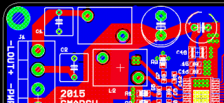
C21/C22 are turned sideways, attached to top layer PVCC/ground planes and shrunk to 8mm diameter, so you'll be stuffing a 100uF/35V or similar polymer cap in that position. C11/C14 will take a higher value wet electrolytic as before.

Contemplating changing C21/C22 to surface mount, as there's a wider selection of parts available versus through-hole.
C21/C22 are turned sideways, attached to top layer PVCC/ground planes and shrunk to 8mm diameter, so you'll be stuffing a 100uF/35V or similar polymer cap in that position. C11/C14 will take a higher value wet electrolytic as before.
Contemplating changing C21/C22 to surface mount, as there's a wider selection of parts available versus through-hole.
Futzed with the TPA decoupling, didn't change anything else yet.
C21/C22 are turned sideways, attached to top layer PVCC/ground planes and shrunk to 8mm diameter, so you'll be stuffing a 100uF/35V or similar polymer cap in that position. C11/C14 will take a higher value wet electrolytic as before.
Contemplating changing C21/C22 to surface mount, as there's a wider selection of parts available versus through-hole.
Nice design Gmarsh! I don't see the post inductor output RF snubber resistor/cap networks. Is it on the underside?
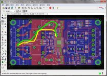
gmarsh, the actual current path is shown in yellow, but you want to have it like green. So the fill must get narrowed at the pin.
Attachments
Last edited:
Don't have a post-inductor snubber - don't really see the need for one as there's no real parasitic resonance at that point that needs to be kept under control.Nice design Gmarsh! I don't see the post inductor output RF snubber resistor/cap networks. Is it on the underside?
- Status
- Not open for further replies.
- Home
- Amplifiers
- Class D
- "Proper" TDA3116 PCB